Draw a circuit diagram to study characteristics of a transistor (pnp or ppn) in common emitter configuration. Draw the sketch of (i) input characterisitics and (ii) output characteristics for this configuration.
Common emitter characteistics. The circuit diagram for common emitter p-n-p transistor is shown in fig.(a). The input is applied across the emitter and base and output is taken across collector and emitter. Here emitter is common to both input and output circuits. The most important characteristics of common base connections are input characteristic and output characteristics.

(i) Input Characteristics
A graph showing the relationship between base-emitter voltage and base-current and constant collector-emitter is called input characteristics of the transistor.
To obtain input characteristic , the emitter is forward biased by base emitter voltage Vbe and the collector is reverse biased by collector emitter voltage Vce. The collector voltage Vec is kept constant at a suitable value. The base voltage Vbe is varied in small steps and the base current Ib is noted corresponding to each value of the base-emitter voltage. A curve is then plotted between Vbc and Ib for a given value of Vce. This is one characteristic. Similar characteristic curves can be drawn for different fixed values of Vce(say−2V,−4Vetc) as shown in fig. (b) .

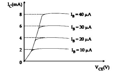
(ii) Output characteristics
. A graph showing the relationship between the collector base voltage and collector current at constant output characteristic of the transistor.
To obtain output characterisitics the base current is kept constant at a suitable value the collector emitter voltage Vce is varied in small steps and the collector current Ic is noted corresponding to each value of the base current Ib . A curve is then plotted between Vce and Ic for a given value Ib. This is one characteristic. Similar characteristic curves can be drawn for different fixed

values of Ib (say 10μA, 15μA, 20μA etc. as shown in fig.(c)
Topper's Solved these Questions
- SOLIDS AND SEMICONDUCTOR DEVICESBOOK - MBD -HARYANA BOARDCHAPTER - SOLIDS AND SEMICONDUCTOR DEVICESEXERCISE - Long answer type questions
6 Videos
- SOLIDS AND SEMICONDUCTOR DEVICESBOOK - MBD -HARYANA BOARDCHAPTER - SOLIDS AND SEMICONDUCTOR DEVICESEXERCISE - Objective type questions
21 Videos
- SOLIDS AND SEMICONDUCTOR DEVICESBOOK - MBD -HARYANA BOARDCHAPTER - SOLIDS AND SEMICONDUCTOR DEVICESEXERCISE - Objective type questions
21 Videos
- PRINCIPLES OF COMMUNICATIONBOOK - MBD -HARYANA BOARDCHAPTER - PRINCIPLES OF COMMUNICATIONEXERCISE - Objective Type Questions
19 Videos
Similar Questions
Draw a circuit diagram to obtain the characteristics of a n-p-n transistor in common base configuration . Give shape of input and output characteristic curves.
View SolutionDefine the dynamic output resistance of a transistor amplifier in common - emitter configuration.
View Solution(i) Draw a circuit diagram to study the input and output characteristics of an n-p-n transistor in its common emitter configuration. Draw the typical input and output characteristics.
(ii) Explain, with the hepl of a circuit diagram, the working of n-p-n transistor as a common emitter amplifier.
View SolutionDraw a circuit diagram to study characteristics of n-p-n transistor in CE configuration. Draw the sketch of input and output characteristics of this configuration . Define current amplification factor ?
View Solution(i) Write the functions of three segments of a transistor.
(ii) Draw the ciruit diagram or studying the input and output characteristics of n-p-n transisfor in common emitter configuration . Using the circuit explain how input characteristics are obtained .
View SolutionThe typical output characteristics curve for a transistor working in the common-emitter configuration is shown in the figure.

View SolutionDraw the circuit diagram for studying the characteristics of a transistor in common emitter configuration. Explain briefly and show how input and output characteristics are drawn.
View SolutionDraw the circuit diagram for studying the characteristics of a transistor in common emitter configuration. Explain briefly and show how input and output characteristics are drawn.
View Solution(a) Draw the circuit arrangement for studying the input and output characteristics of an n-p-n transistor in CE configuration . With the help of these characteristics define (i) input resistance , (ii) current amplification factor .
(b) Describe briefly with the help of a circuit diagram how an n-p-n transistor is used to produce self-sustained oscillations .
View SolutionDraw typical output characteristics of an n-p-n transistor in CE configuration. Show how these characteristics can be used to determine output resistance.
View Solution
