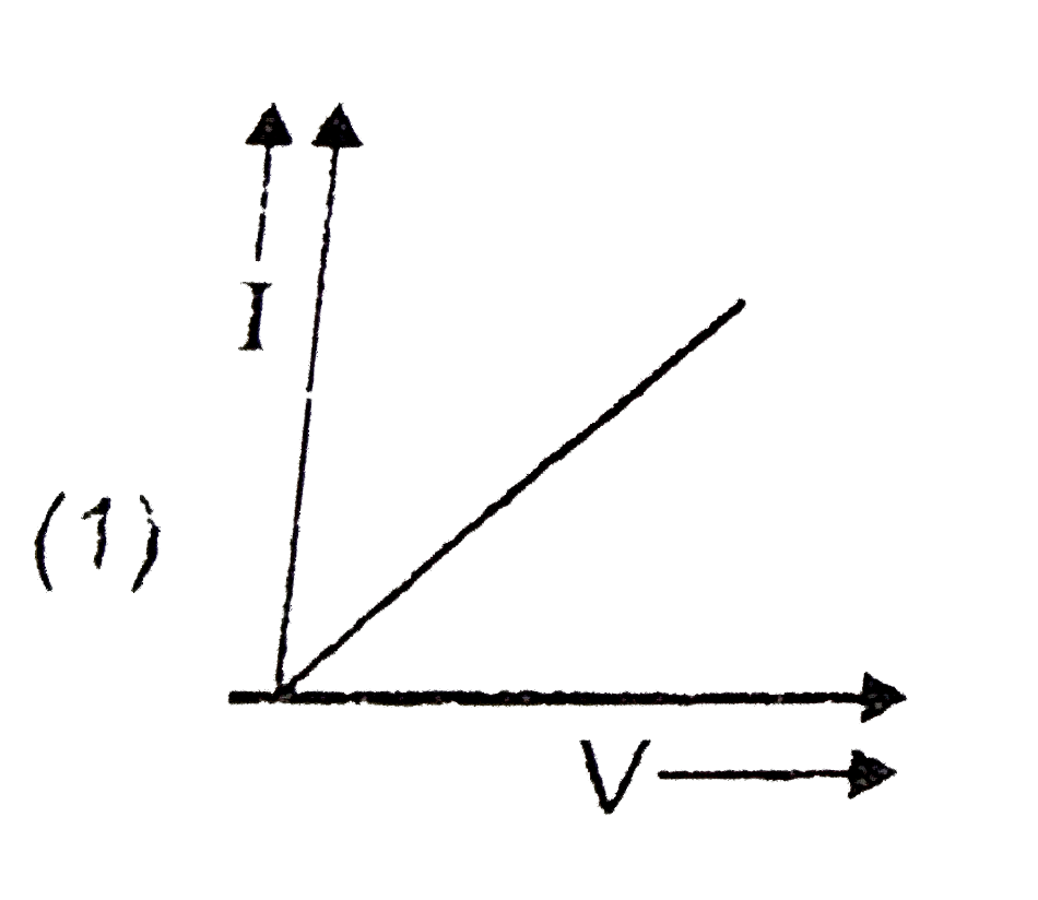
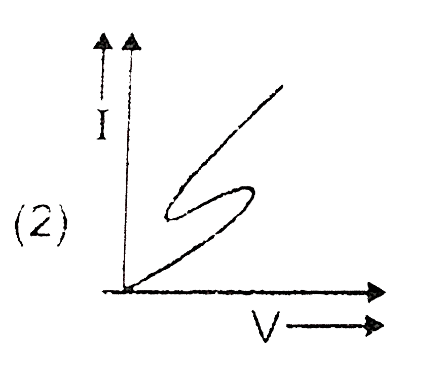
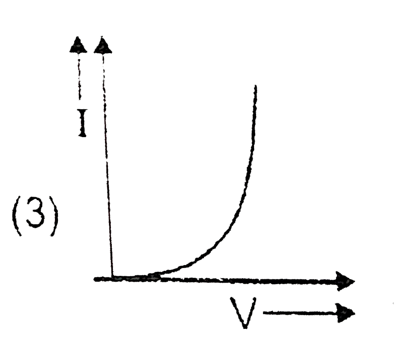
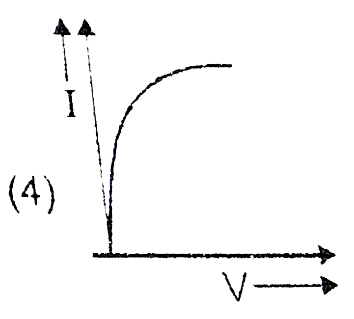
The reverse biased characteristics of a p-n junction are :


The correct Answer is:C
Topper's Solved these Questions
- SOLIDS & SEMICONDUCTOR DEVICESBOOK - MODERN PUBLICATIONCHAPTER - SOLIDS & SEMICONDUCTOR DEVICESEXERCISE - Recent Competitive Questions
26 Videos
- ROTATIONAL MOTIONBOOK - MODERN PUBLICATIONCHAPTER - ROTATIONAL MOTIONEXERCISE - RCQ
8 Videos
- TRANSFERENCE OF HEAT BOOK - MODERN PUBLICATIONCHAPTER - TRANSFERENCE OF HEAT EXERCISE - Recent Competitive Questions
4 Videos
Similar Questions
Choose the correct option for the forward biased characteristics of a p-n junction
View SolutionUsing the necessary circuit diagram, show how the V-I characteristics of a p-n junction are obtained in (i) forward biasing (ii) Reverse biasing. How are these characteristics made use of in rectification?
View Solution
Knowledge Check
In which one of the following devices the reverse biased characteristics of a p-n junction diode are used?
AAmplifierBZener diodeCOscillatorDLogic gateChoose the correct option for the forward biased characteristics of a p-n junction
A B
B C
C D
D
In V- I characteristics of p−n junction in reverse biasing results in
Aleakeage currentBthe current which cannot be neglectedCno flow of currentDlarge current
Using the necessary circuit diagram, show how the V-I characteristics of a p-n junction are obtained in (i) forward biasing (ii) Reverse biasing. How are these characteristics made use of in rectification?
View SolutionUsing the necessary circuit diagram, show how the V-I characteristics of a p-n junction are obtained in (i) forward biasing (ii) Reverse biasing. How are these characteristics made use of in rectification?
View SolutionAssertion: In reverse biased condition a p-n junction diode does not conduct.
Reason: In reverse biased condition a diode has zero resistance.
View SolutionAssertion: In reverse biased condition a p-n junction diode does not conduct.
Reason: In reverse biased condition a diode has zero resistance.
View SolutionAssertion:The dominant mechanism for motion of charge carriers in forward and reverse biased silicon P−N junction are drift in both forward and reverse biase.
Reason: In reverse biasing, no current flow through the junction.
View Solution
