What are 1) forward bias and 2) reverse - bias?
Step-by-Step Solution:
1. Understanding P-N Junction Diode:
- A P-N junction diode is formed by joining a p-type semiconductor (which has an abundance of holes) with an n-type semiconductor (which has an abundance of electrons).
2. Forward Bias:
- In forward bias, the positive terminal of an external voltage source is connected to the p-side (p-type semiconductor) and the negative terminal is connected to the n-side (n-type semiconductor).
- This connection reduces the potential barrier at the junction, allowing current to flow easily through the diode. The electric field created by the external voltage opposes the built-in electric field of the diode, effectively allowing charge carriers (holes and electrons) to recombine and conduct electricity.
3. Reverse Bias:
- In reverse bias, the connections are reversed: the positive terminal of the voltage source is connected to the n-side and the negative terminal is connected to the p-side.
- This increases the potential barrier at the junction, preventing current from flowing through the diode. The external electric field reinforces the built-in electric field of the diode, widening the depletion region and effectively blocking the flow of charge carriers.
4. Electric Field Direction:
- In forward bias, the external electric field is in the same direction as the built-in electric field of the diode, which allows current to flow.
- In reverse bias, the external electric field is in the opposite direction to the built-in electric field, which prevents current flow.
Summary:
- Forward Bias: Positive terminal to p-side, negative terminal to n-side, allowing current flow.
- Reverse Bias: Positive terminal to n-side, negative terminal to p-side, blocking current flow.
---
- A P-N junction diode is formed by joining a p-type semiconductor (which has an abundance of holes) with an n-type semiconductor (which has an abundance of electrons).
- In forward bias, the positive terminal of an external voltage source is connected to the p-side (p-type semiconductor) and the negative terminal is connected to the n-side (n-type semiconductor).
- This connection reduces the potential barrier at the junction, allowing current to flow easily through the diode. The electric field created by the external voltage opposes the built-in electric field of the diode, effectively allowing charge carriers (holes and electrons) to recombine and conduct electricity.
- In reverse bias, the connections are reversed: the positive terminal of the voltage source is connected to the n-side and the negative terminal is connected to the p-side.
- This increases the potential barrier at the junction, preventing current from flowing through the diode. The external electric field reinforces the built-in electric field of the diode, widening the depletion region and effectively blocking the flow of charge carriers.
- In forward bias, the external electric field is in the same direction as the built-in electric field of the diode, which allows current to flow.
- In reverse bias, the external electric field is in the opposite direction to the built-in electric field, which prevents current flow.
- Forward Bias: Positive terminal to p-side, negative terminal to n-side, allowing current flow.
- Reverse Bias: Positive terminal to n-side, negative terminal to p-side, blocking current flow.
Topper's Solved these Questions
- SEMICONDUCTOR DEVICESBOOK - AAKASH SERIESCHAPTER - SEMICONDUCTOR DEVICESEXERCISE - Problems (LEVEL-I)
35 Videos
- SEMICONDUCTOR DEVICESBOOK - AAKASH SERIESCHAPTER - SEMICONDUCTOR DEVICESEXERCISE - Problems (LEVEL-II)
9 Videos
- SEMICONDUCTOR DEVICESBOOK - AAKASH SERIESCHAPTER - SEMICONDUCTOR DEVICESEXERCISE - Exercise (Short answer questions)
27 Videos
- RAY OPTICSBOOK - AAKASH SERIESCHAPTER - RAY OPTICSEXERCISE - PROBLEMS ( LEVEL-II)
60 Videos
- UNITS AND MEASUREMENTBOOK - AAKASH SERIESCHAPTER - UNITS AND MEASUREMENTEXERCISE - PRACTICE EXERCISE
45 Videos
Similar Questions
Knowledge Check
The dominant mechanisms for motion of charge carriers in forward and reverse biased silicon P−N junction are
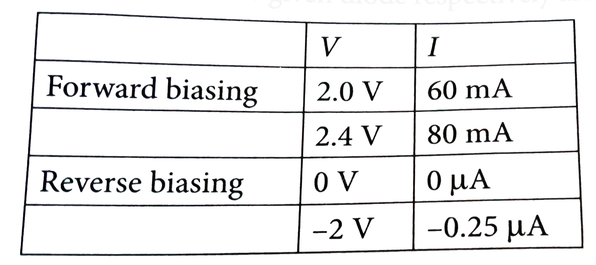
Adrift in forward bias, diffusion in reverse biasBdiffusion in forward bias, drift in reverse biasCdiffusion in both forward and reverse biasDdrift in both forward and reverse biasThe following table provides the set of values of V and I obtained for a given diode. Let the characteristics α be nearly linear, over this range, the forward and reverse bias resistance of the given diode respectively are
 A10Ω,8×106ΩB20Ω,4×105ΩC20Ω,8×106ΩD10Ω,10Ω
(i) Figure shows the input waveform which is converted by a device .X. into an output wavefrom. Mane the device and explain its working using the proper circuit.
(ii) Draw the forward bias and reverse blas circuit for the basic component of the device and draw the characterstics.
Explain clearly which region of the curve is used in an amplifier.
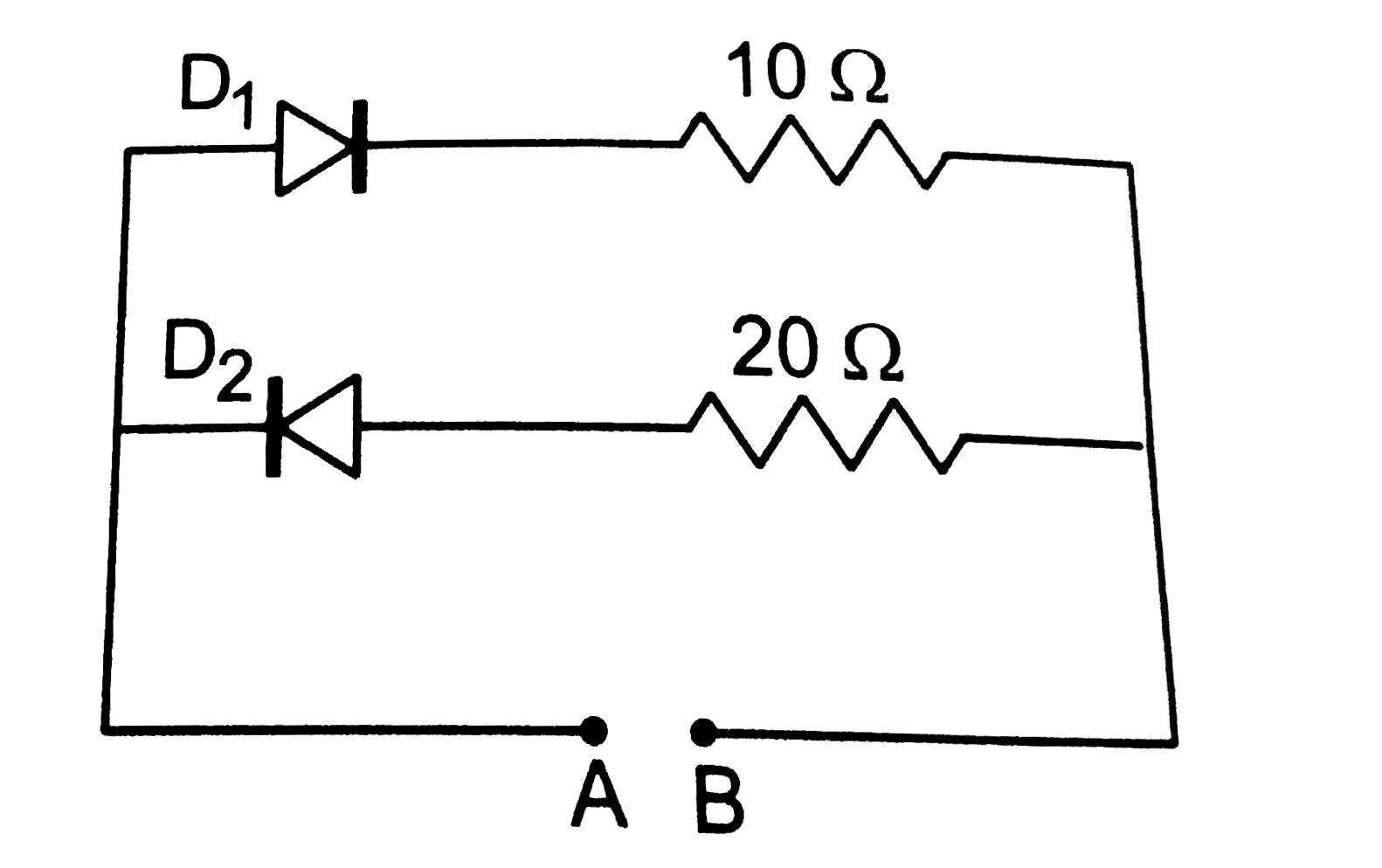
View SolutionA 2V battery may be connected across the points A and B as shown in figure. Assume that the resistance of each diode is zero in forward bias and infinity in reverse bias.Find the current supplied by the battery if the positive terminal of the battery is connected to (a) the point A (b)the point B.

View SolutionWith reference to a semi-conductor diode, what is meant by : (i) Forward bias
(ii) Reverse bias
(iii) Depletion region.
(b) An EM wave, Y1, has a wavelength of 1 cm while another EM wave, Y2, has a frequency of 1015 Hz. Name two type of waves and write one application for each.
View SolutionWhat is the ratio of forward and reverse resistance of p-n junction diode?
View SolutionThe resistance of p-n junction is low when forward biased and is high when reverse biased. Explain.
View SolutionFor the equilibrium A⇔B , the variation of the rate of the forward (a) and reverse (b) reaction with time is given by :
View Solution

