Complete Solutions to C.U.Q (INTRINSIC AND EXTRINSIC SEMICONDUCTORS) of chapter SEMICONDUCTOR ELECTRONICS of Class 12 book with complete answers and questions
| Class 12 | PHYSICS |
| Chapter | SEMICONDUCTOR ELECTRONICS |
| NARAYANA | C.U.Q (INTRINSIC AND EXTRINSIC SEMICONDUCTORS) |
| Number Of Questions | 70 |
| Academic Year | 2023-24 |
In semiconductors at a room temperature
02:00View SolutionIn a `n`-type semiconductor, which of the following statement is true?
02:09View SolutionCarbon silicon and germanium have four valence electrons each. These are characterised by valence and conduction bands separated by energy band gap respectively equal to `(E_(g))_(C), (E_(g))_(Si) " ""and" " "(E_(g))_(Ge)` which of the following statements is true?
04:48View SolutionIdentify the property which is not characteristic for a semiconductor ?
03:00View SolutionCarbon , silicon and germanium have four valence electrons each . At room temperature which one of the following statements is most appropriate ?
02:14View SolutionWhen phosphorus and antimony are mixed in germanium, then
01:30View SolutionAn electrically neutral semiconductor has
02:12View SolutionThere is no hole current in conductors because they have
01:33View SolutionIn the insulators
02:27View SolutionIn semiconductors the for bidden energy gap between `V.B` and `C.B` is of the order of
02:31View SolutionThe level formed due to impurity atom, in the for hidden energy gap, very near to the valence band in a p-type semiconductor is called
02:40View SolutionThe bond in semiconductors is
02:14View SolutionOn increasing temperature, the conductivity of pure semiconductors
02:37View SolutionThe mobility of free electrons is greater then that of free holes because
02:56View SolutionA semiconductor at `0 K` behaves as
02:09View SolutionThe valency of impurity element for making p-type semiconductors is
02:28View SolutionIn n-type semiconductors the electron concentration is equal to
03:50View SolutionWhich of the following statement is not true ?
View Solutionp-type semi conduor is
View SolutionAn n-type semi- conductor is
01:27View SolutionAn electric field is applied across a semiconductor. Let `n` be the number of charge carries. As temperature increases, `n` will
01:25View SolutionIn a n-type semiconductor, the femi energy level lies
03:09View SolutionAn n-type and p-type silicon can be obtained by doping pure silicon with.
03:21View SolutionThe width of forbidden gap in silicon crystal is `1.1 eV`. When the crystal is converted into a `N`-type semiconductor the distance of Fermi level from conduction band is
03:51View SolutionIn extrinsic semiconductors
01:46View SolutionThe element that can be used as acceptor impurity to dope silicon is
01:26View SolutionAmong the following, the wrong statement on the case of semiconductor is
02:29View SolutionThe value indicated by fermi energy level in an intrinsic semiconductor is
02:17View SolutionThe conduction band and valency band of a good conductors are
02:36View SolutionTwo pieces one of germinium and the other of aluminium are cooled from `T_(1) K` to `T_(2) K`. The resistance of
02:51View SolutionIn intrinsic semiconductor at room temperature the no. of electrons and holes are
01:10View SolutionBand gap in insulator is of the order
02:09View SolutionIn p-type semiconductor conduction in due to
01:47View SolutionIn an intrinsic semiconductor, the fermi energy level is
02:53View SolutionWith increase in temperature in an intrinsic semiconductor the ration of conduction electrons and holes is
02:08View SolutionTo obtain n-type extrinsic semiconductor, the impurity element to be added to germanium should be of valency
02:43View SolutionWhat are the majority carriers in a p-type semiconductor?
04:10View SolutionThe objective of adding impurities in the extrinsic semiconductor is
04:43View SolutionIn intrinsic semiconductor conductivity is due to.
02:00View SolutionIn intrinsic semiconductor conductivity is due to.
02:00View SolutionWhen the conductivity of a semiconductor is only due to breaking of covalent bonds, the semi conductor is called.
02:24View SolutionThe potential barrier at `PN` junction is due to
02:28View SolutionA `PN` junction diode cannot be used
03:11View Solution`p-n` junction diode acts as
02:18View SolutionOn increasing reverse voltage in a `p-n` junction diode the value of reverse current will
02:58View SolutionIn forward bias the depletion layer behaves like
02:58View Solution`p-n` junction in reverse bias behaves like
02:48View SolutionThe main cause of avalence breakdown is
01:43View SolutionWhen `p-n` junction is forward biased, the current across the junction is mainly due to
02:57View SolutionThe current through any `p-n` junction is due to
(a) drift of charge carriers
(b) diffusion of charge carriers
( c) different concentrations of same type of charge carriers in different regions.
(d) Same concentrations of same type of charge carriers in different regions02:39View SolutionThe thickness of depletion layer is approximately
02:46View SolutionThe depletion region is
02:47View SolutionDiffusion current in a p-n junction is greater than the drift current in magnitude
05:45View SolutionDiode is forward biased and the applied voltage is greater than the potential barrier then
(I) resistance of the junction in the forward bias decreases
(II) potential barrier remains same
(III) width barrier remains decreases
(IV) p-type is at higher potential than the n-type.03:06View SolutionWhen a junction diode is reverse biased, then current called drift current is due to
02:53View SolutionAmong the following one statement is not correct when a junction diode is forward bias
02:21View SolutionConsider the following statement `A` and `B` and identify the correct choice of the given answers
`A:` The width of the depletion layer in a `P-N` junction diode increases in forwards biase
`B:` In an intrinsic semiconductor the fermi energy level is exactely in the middle of the forbidden gap02:48View SolutionThe potential in the depletion layer due to.
02:27View SolutionPickout the incorrect statement regarding reverse saturation current in the `p-n` junction diode.
03:00View SolutionWhen the `p-n` junction diode is reverse biased, the thickness of the depletion layer
03:27View Solution`p-n` junction diode can be used as
02:34View SolutionA `p-n` junction diode is reverse biased. Then
01:49View SolutionIn the middle of the depletion layer of a reverse - biased `p - n ` junction , the
04:48View SolutionWhen `p-n` junction diode is forward biased then
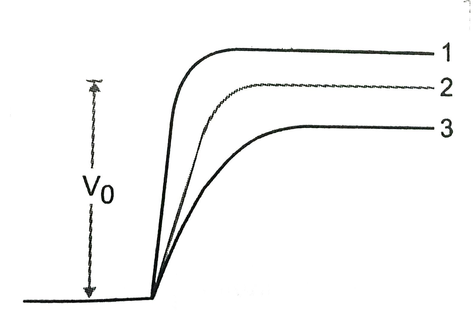
02:59View SolutionIn Fig . `V_(0)` is the potential barrier across a p-n junction, when no battery is connected across the junction
 03:35View Solution
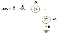
In Fig assuming the diodes to be ideal :
 View Solution
A `Si` and a `Ge` diode has identical physical dimensions. The band gap in `Si` is larger than that in `Ge`. An indentical reverse bias is applied across the diodes.
01:39View SolutionThe correct curve between potential `(V)` and distance `(d)` near `p-n` junction is.
03:09View SolutionWhich of the following is reverse biased diode?
01:34View SolutionIn the case of forward biasing of `PN`-junction, which one of the following figures correctly depicts the direction of flow of carriers?
02:02View Solution
C.U.Q (INTRINSIC AND EXTRINSIC SEMICONDUCTORS) questions and complete solutions for chapter SEMICONDUCTOR ELECTRONICS of NARAYANA PHYSICS (HINGLISH) of Class 12
All Exercises from NARAYANA Class 12 PHYSICS SEMICONDUCTOR ELECTRONICS
- ADDITIONAL EXERCISE (ASSERTION AND REASON TYPE QUESTIONS :)
- C.U.Q (APPLICATION OF JUNCTION DIODE AS RECTIFIER)
- C.U.Q (INTRINSIC AND EXTRINSIC SEMICONDUCTORS)
- C.U.Q (LOGIC GATES)
- C.U.Q (SPECIAL PURPOSE P-N JUNCTION DIODES)
- EVALUATE YOURSELF-1
- EVALUATE YOURSELF-2
- EVALUATE YOURSELF-3
- EVALUATE YOURSELF-4
- EXERCISE -1 (C.W) (APPLICATION OF JUNCTION DIODE AS RECTIFIER)
- EXERCISE -1 (C.W) (INTRINSIC AND EXTRINSIC SEMICONDUCTORS)
- EXERCISE -1 (C.W) (JUNCTION DIODE)
- EXERCISE -1 (C.W) (LOGIC GATES)
- EXERCISE -1 (C.W) (TRANSISTORS)
- EXERCISE -1 (H.W) (APPLICATION OF JUNCTION DIODE AS RECTIFIER
- EXERCISE -1 (H.W) (INTRINSIC AND EXTRINSIC SEMICONDUCTORS)
- EXERCISE -1 (H.W) (JUNCTION DIODE)
- EXERCISE -1 (H.W) (LOGIC GATES)
- EXERCISE -1 (H.W) (TRANSISTORS)
- EXERCISE -2 (C.W) (APPLICATIONS OF JUNCTION DIODE AS RECTIFIER)
- EXERCISE -2 (C.W) (JUNCTION DIODES)
- EXERCISE -2 (C.W) (LOGIC GATES)
- EXERCISE -2 (C.W) (TRANSISTORS)
- EXERCISE -2 (C.W) INTRINSIC, EXTRINSIC SEMICONDUCTONS)
- EXERCISE -2 (H.W) (APPLICATIONS OF JUNCTION DIODE AS RECTIFIER)
- EXERCISE -2 (H.W) (INTRINSIC, EXTRINSIC SEMICONDUCTORS)
- EXERCISE -2 (H.W) (JUNCTION DIODES)
- EXERCISE -2 (H.W) (LOGIC GATE)
- EXERCISE -2 (H.W) (TRANSISTORS)
- EXERCISE -3
- EXERCISE-4
- ILLUSTRATION
