Complete Solutions to Exercise of chapter ELECTRONIC DEVICES of Class 12 book with complete answers and questions
| Class 12 | PHYSICS |
| Chapter | ELECTRONIC DEVICES |
| PRADEEP | Exercise |
| Number Of Questions | 100 |
| Academic Year | 2023-24 |
Distinguish between conductor (or metals), semiconductors and insulators on the basis of theur energy bands.
02:44View SolutionWhat are the Instrinsic semiconductor ? Explain how do they work?
02:21View SolutionWhat do you understand by term 'holes' in a semiconductor? Discuss how they move under the influence of an electric field?
01:37View SolutionDiscuss electrical conduction in semiconductors.
03:52View SolutionWhat is doping ? State the methods of doping.
03:06View SolutionHow is an n-type semiconductor formed? Name the majority charge carriers in it. Draw the energy band diagram of n-type semiconductor.
03:06View SolutionDraw the energy band diagram of a p-type semiconductor. Deduce an expression for the conductivity of a p-type semiconductor.
09:17View SolutionEFFECT OF TEMPERATURE ON THE MOBILITY AND CONDUCTIVITY OF ELECTRONS AND HOLES
02:20View SolutionWhat do you understand by electrical conductivity of a semiconductor? Find a relation for the same.
08:02View SolutionWhat is p-n junction? How is a p-n junction made? How potential barrier is caused in it.
05:17View SolutionExplain the formation of depletion layer and potential barrier in p-n junction.
Draw the circuit diagram of a half wave rectifier and explain its working.15:26View SolutionExplain with the help of a diagram, how depletion region and potential barrier are formed in a junction diode.
If a small voltage is applied to a p-n junction diode how will the barrier potential be affected when it is (i) forward biased and (ii) reverse biased?05:52View SolutionUsing the necessary circuit diagram, show how the V-I characteristics of a p-n junction are obtained in (i) forward biasing (ii) Reverse biasing. How are these characteristics made use of in rectification?
06:21View SolutionExplain briefly with the help of necessary diagram, the forward and the reverse biasing of p-n junction diode. Also draw their characteristic curves in the two cases.
10:02View SolutionDraw a circuit diagram of a full-wave rectifier. Explain its working principle. Draw the input/output wave forms indicating clearly the function of the two diode used.
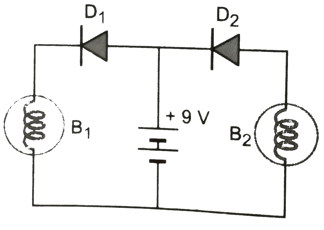
09:40View SolutionIn the following diagram, which bulb out of `B_(1)` and` B_(2)` will glow and why?
Draw a diagram of an illuminated p-n junction solar cell
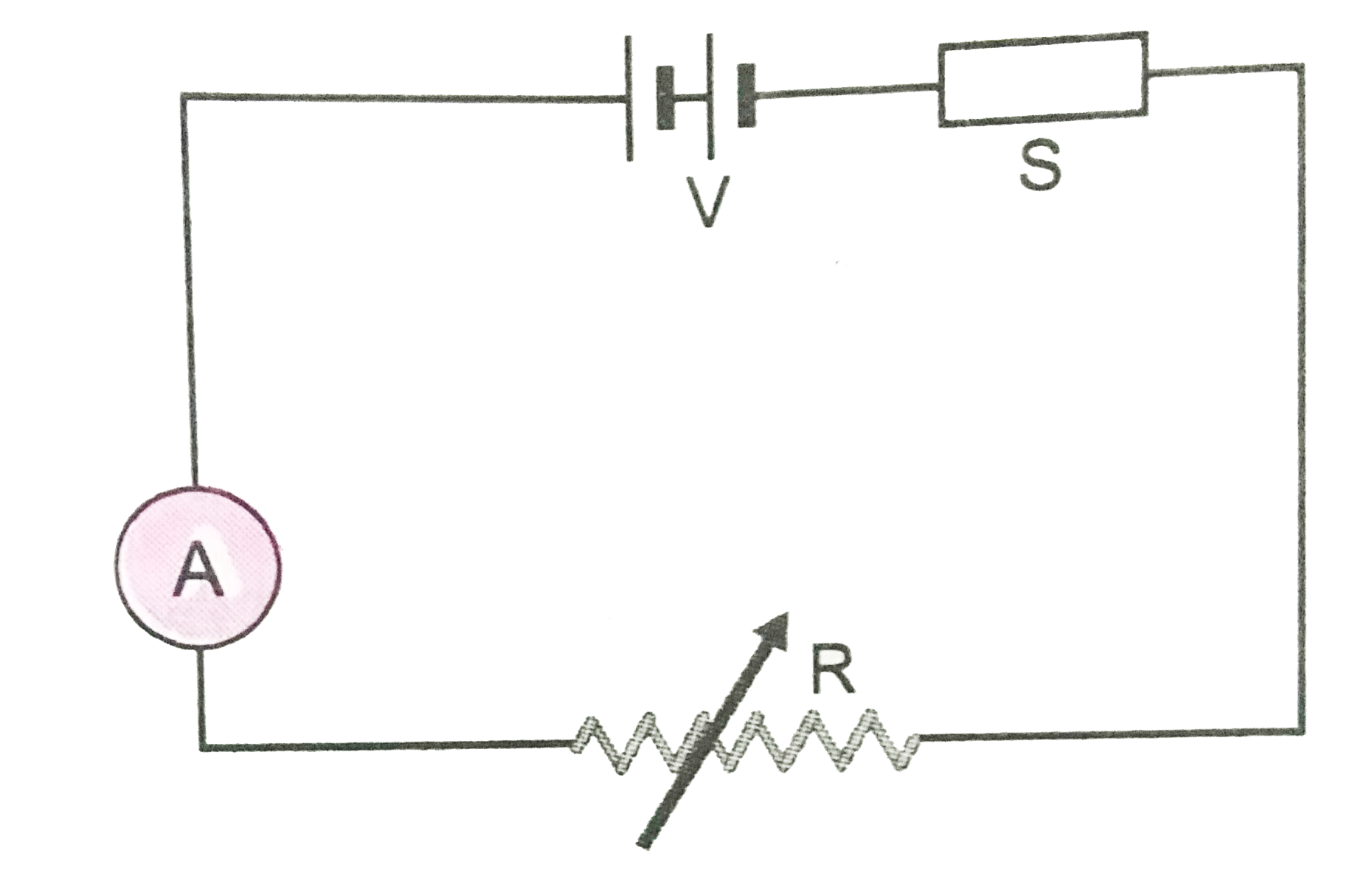
Explain briefly the three processes due to which generation of emf takes place in a solar cell.03:20View SolutionThe diagram Fig.12 shown a piece of pure semiconductor S in series with a variable resistor R, and a source of constant voltage V. Would you increase or decrease the value of R to keep the reading of ammeter constant, when semi-conductor S is heated? Give reason.
 01:51View Solution
Draw the circuit diagram of an illuminated photodiode in reverse bias? How is photodiode used to measure light intensity?
03:36View SolutionWhat is light emitting diode (LED) ? Mention two important advantages of LEDs over con-ventional lamps.
02:20View SolutionMention the important considerations required while fabricating a p-n junction diode to be used as light emitting diode (LED). What should be the order of the band gap of an LED if it is required to emit light in the visible region.
01:46View SolutionGive reasons for the following:
(i) High reverse voltage do not appear across a LED. (ii) Sunlight is always required for the working of a solar cell.
(iii) The electric field, of the junction of a ener diode, is very high even for a small reverse bias voltage of about 5V.04:46View SolutionWrite the function of three segments of a transistor.
View SolutionSketch the three modes of study of n-p-n junction transistor.
06:48View SolutionExplain that a transistor can be used as a switch.
02:45View SolutionDiscuss briefly the concept of an amplifier.
04:28View SolutionDraw a circuit diagram of a transistor amplifier in CE configuration. Define the terms (i) Input resistance and (ii) Current amplification factor. How are these determined using input and output characteristics?
09:34View SolutionExplain the advantages and disadvantages of semiconducting devices compared to vacuum tube.
03:03View SolutionGive the logic symbol, truth table and Boolean expression for OR gate. How is it realised in practice?
03:47View SolutionGive the logic symbol, truth table and Boolean expression for AND gate? How is it obtained in practice?
02:34View SolutionHow is NOT gate realised? Explain.
08:13View SolutionWhat is logic gate? Distinguish between AND and OR gates.
02:22View SolutionWhat are main logic gates? How many types are they? Draw their symbols and truth tables.
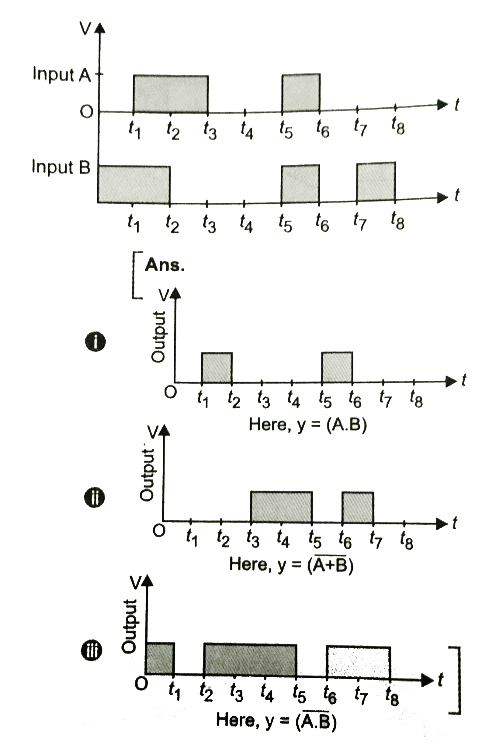
02:15View SolutionTwo signals A, B as given below are applied to (i) AND (ii) NOR and (iii) NAND gates. Draw the output wave form in each case.
 06:50View Solution
Give the logic symbol, Boolean expression and truth table of NAND gate.
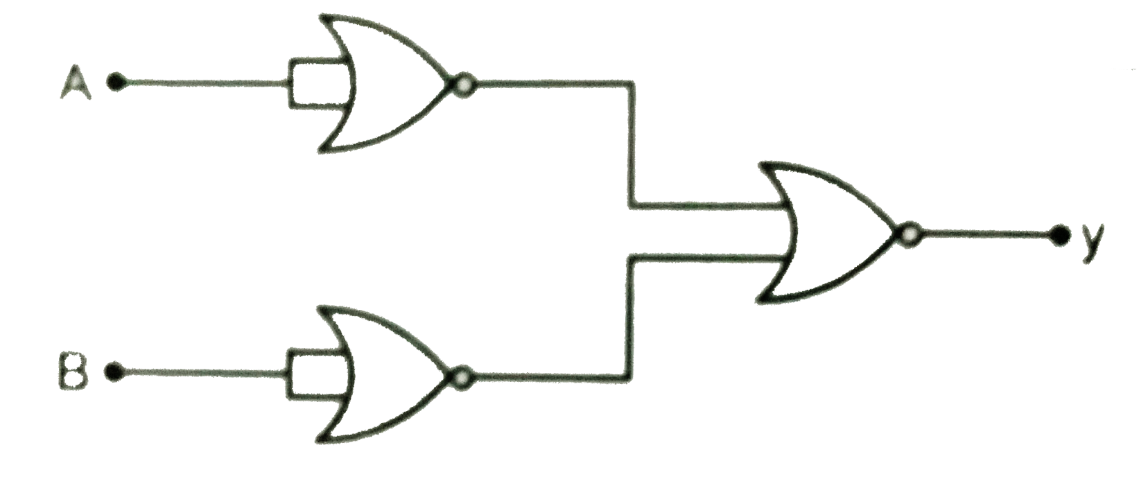
01:19View SolutionIdentify the logic gate equivalent to the circuit shown in the Fig.Draw the truth table for all possible values of inputs A and B.
 03:18View Solution
Discuss an integrated circuit. Explain the meaning of SSI, MSI, LSI and VLSI.
02:19View SolutionWhat is integrated circuit ? Discuss the advantages of integrated circuit over conventional electronic circuit.
01:58View SolutionExplain formation of energy band in solids. Distinguish between conductors, extrinsic and intrinsic semi-conductors and insulators on the basis of band theory.
08:11View SolutionDraw the "energy bands" diagram for a (i) pure semiconductor (ii) insulator. How does the energy band, foe a pure semiconductor, get affected when this semiconductor is doped with an acceptor impurity donor impurity? Hence discuss why the 'holes' and the 'electrons' respectively, become the 'majority charge carriers' in these two cases.
09:32View SolutionWhat is an extrinsic semiconductor? Discuss the working of the various types of extrinsic semiconductors with help of their energy band diagram.
04:54View SolutionDistinguish between (i) Intrinsic and Extrinsic semiconductor and
(ii) n-type semiconductor and p-type semi-conductor.03:49View SolutionDistinguish between n-type and p-type semiconductors on the basis of energy-band diagrams. Explain the process of conduction in both type of materials.
06:38View SolutionDraw a circuit diagram of a full-wave rectifier. Explain its working principle. Draw the input/output wave forms indicating clearly the function of the two diode used.
09:40View SolutionExplain (i) forward biasing (ii) reverse biasing of a P-N junction diode. With the help of a circuit diagram, explain the use of this device as a half wave rectifier.
10:29View SolutionWhat is a p-n junction diode? Define the term 'dynamic resistance' for the junction diode. With the help of a circuit diagram explain the working of a p-n junction diode as a full wave rectifier.
09:47View SolutionWhat do you understand by decimal number system and binary number system. Discuss conversion of decimal number system into binary number system with illustrations.
08:11View SolutionWhat do you understand by logic gate? Why is it so called? State the type of gates.
02:35View SolutionDescribe (i) NAND gate, (ii) NOR gate and (iii) XOR gate.
05:40View SolutionExplain how an OR gate may be constructed with AND and NOT gates. A logic circuit is given in the Fig.charge it in simpler form.
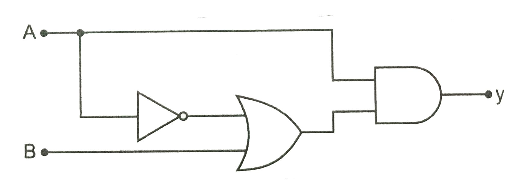
[Refer to conceptual Problem 4 for first part. The given figure represents AND gates as `y=A.(barA(A+B))=A.barA+A.B=A.B]`02:19View SolutionA semiconductor has equal electron and hole concentration of `6xx10^(8)//m^(3)`. On doping with certain impurity, electron concentration increases to `9xx10^(12)//m^(3)`. (i) Identify the new semiconductor obtained after doping. (ii) Calculate the new hole concentration. (iii) How does the energy gap vary with doping?
03:00View SolutionIn a pure semiconductor, the number of conduction electrons is `6xx10^(19)` per cubic metre. Find the total number of current carriers (electrons and holes) in a same semiconductor of size `1cmxx1cmxx1mm`.
03:08View SolutionA p-type semiconductor has acceptor energy level 53meV above the valence band. Find the maximum wavelength of light that can creat a hole. Use `h=6.63xx10^(-34)Js, c=3xx10^(8)ms^(-1)`.
01:53View SolutionThe electrical conductivity of a semiconductor increases when electromagnatic radiation of wavelength shorter than 2480 nm is incident on it. Find the band gap of the semiconductor. Given `h=6.63xx10^(-34)Js, and 1eV=1.6xx10^(-19)J`.
01:47View SolutionA doped semiconductor has impurity levels 20 meV below the conduction band. Is the material n-type or p-type? What is the wavelength of light so that the electron of impurity level is just able to jump into conduction band?
Use `h=6.63xx10^(-34)Js, c=3xx10^(8)m//s`.02:32View SolutionPure `Si` at `500K` has equal number of electron `(n_(e))` and hole `(n_(h))` concentration of `1.5xx10^(16)m^(-3)`. Dopping by indium. Increases `n_(h)` to `4.5xx10^(22) m^(-3)`. The doped semiconductor is of
03:07View SolutionFind the number density of impurity atoms that must be added to a pure silicon crystal inorder to convert it to have resistivity (i) `10^(-1)Omegam` n-type silicon (ii) `10^(-1)Omegam` p-type silicon. Give for silicon: `mu_(e)=0.135m^(2)V^(-1)s^(-1)`
and `mu_(h)=0.048m^(2)V^(-1)s^(-1)`.03:32View SolutionDetermine the number density of donor atoms which have to be added to an intrinsic germanium semiconductor to produce an n-type semiconductor of conductivity `5Omega^(-1)cm^(-1)`, given that the mobility of electron in n-type germanium is `3900 cm^(2)V^(-1)s^(-1)`. Neglect the contribution of holes to conductivity.
03:21View SolutionOn doping germanium with donor atoms of density `10^(17)cm^(-3)`, find its conductivity if mobility of electrons is `3800 cm^(2)//V-s` and intrinsic carrier concentration is `2.5xx10^(13)cm^(-3)`. Also find the ratio of conductivity of doped germanium and pure germanium.
03:07View SolutionThe energy of a photon of sodium light wavelength `5890 Å` equals the energy gap of a semiconducting material. Find the minimum energy E required to create a hole-electron combination. the value of `E//kT` at a temperature of `27^(@)C`, where `k=8.62xx10^(-5) eV//K, h=6.63xx10^(-34)Js`.
02:59View SolutionCalculate the number of states per cubic metre of sodium in 3s band. The density of sodium is `1013kgm^(-3)`.How naby of them are empty?
05:15View SolutionFind the current produced at room temperature in a pure germanium plate of area `2 xx 10^(-4) m^(2)` and of thickness `1.2 xx 10^(-3) m` when a potential of `5 V` is applied across the faces. Concentration of carries in germanium at room temperature is `1.6 xx 10^(6)` per cubic metre. The mobilities of electrons and holes are `0.4 m^(2) V^(-1) s^(-1)` and `0.2 m^(2) V^(-1) s^(-1)` respectively. The heat energy generated in the plate in `100` second is.
04:37View SolutionIf resistivity of pure silicon is `3000 Omega meter`, and the electron and hole mobilities are `0.12 m^(2)V^(-1)s^(-1)` and `0.045m^(2)V^(-1)s^(-1)` respectively, determine the resistivity of a specimen of the material when `10^(19)` atoms of phosphorous are added per `m^(3)` are also added. Given charge on electron `=1.6x10^(-19)C`.
04:32View SolutionThe V-I characteristics of a silicon diode is given in Fig .Calculate the diode resistance in
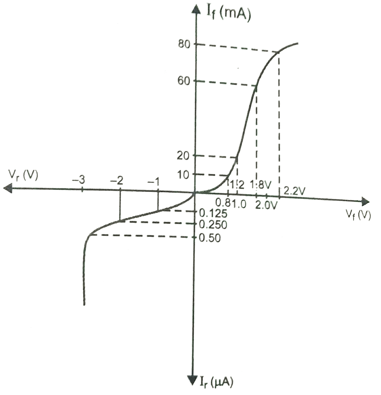
forward bias at `V=+2V` and `V=+1V` and
reverse bias `V=-1V` and `V=-2V`.04:54View SolutionA p-n junction is fabricated from a semiconductor with band gap of `3.0 eV`. Can it detect a wavelength of (i) `600nm` (ii)`400nm`?
Given, `h=6.6xx10^(-34)Js`.03:14View SolutionThe width of depletion region in a P-N junction diode is 500 nm and an intense electric field of `5xx10^(5)Vm^(-1)` is also found to exit init. Determine the height of the potential barrier. Also calculate the kinetic energy which a conduction electron must have inorder to diffuse from the n-side to p-side.
02:28View SolutionCalculate the current through the circuit and the potential difference across the diode shown in Fig. The drift current for the diode is `30muA`.
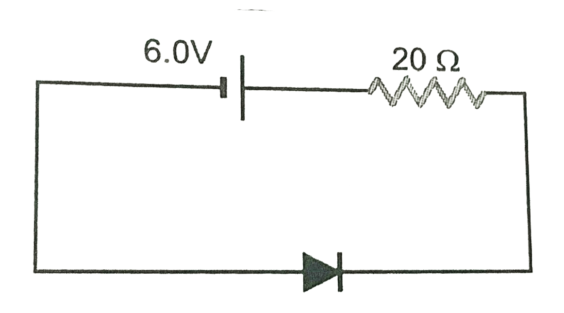 02:17View Solution
A sinusoidal voltage of rms value 200 volt is connected to a diode and a resistor R in the circuit as shown in Fig., so that half wave rectification occurs. If the diode is ideal, what is the rms voltage across R? If resistor R is replaced by capactior of capacitance C, find the potential difference across C.
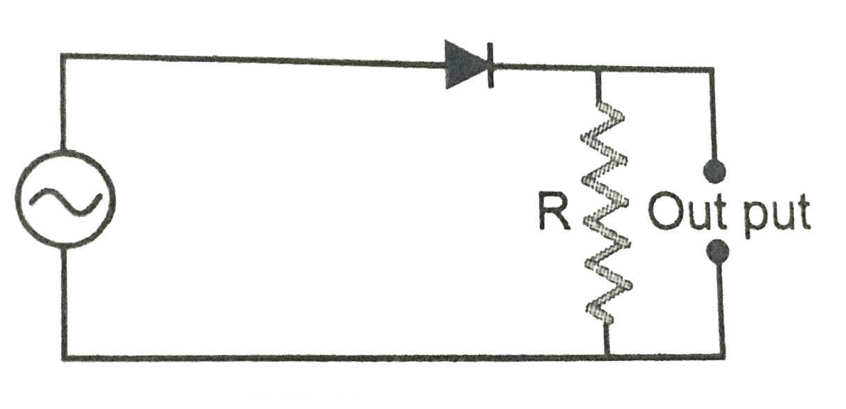 02:41View Solution
Find the current through the resistance R in Fig if `R =10 Omega` and `R=20Omega`.
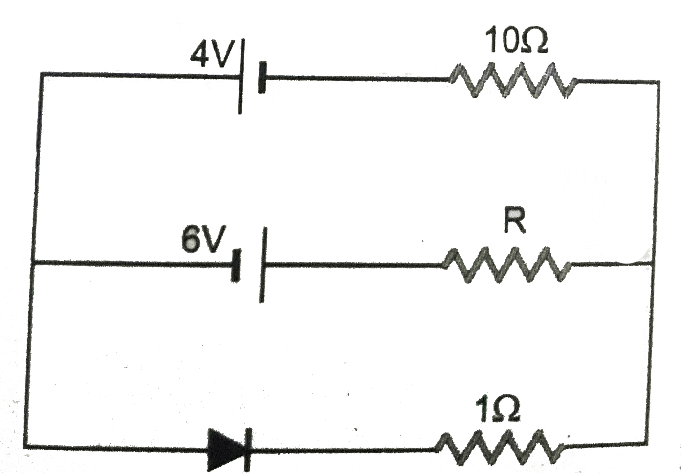 04:00View Solution
A silicon p-n junction diode whose knee voltage is `0.7 V` is connected to a battery with supply voltage `3V` and `100mA` in forward biasing. If a resistor R is used in series of the circuit, then a current of 20mA passes through the diode. Find the wattage of the resistor and of the diode.
03:11View SolutionAssuming that the resistance of the meters are negligible, what will be the readings of the ammeters `A_(1)` and `A_(2)` in the circuit shown in Fig.
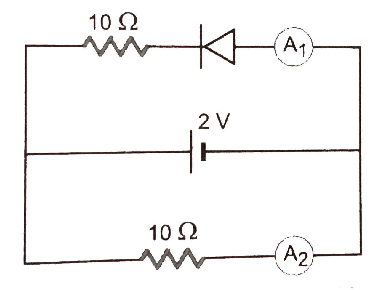 03:14View Solution
The applied input a.c. to a half wave rectifier is 120 watt. The d.c. output is 50 watt. What is the rectification effeciency and power effeciency?
02:55View SolutionFind the average value of d.c. voltage that can be obtained from the half wave rectifier of Fig. assuming that the diode is ideal one.
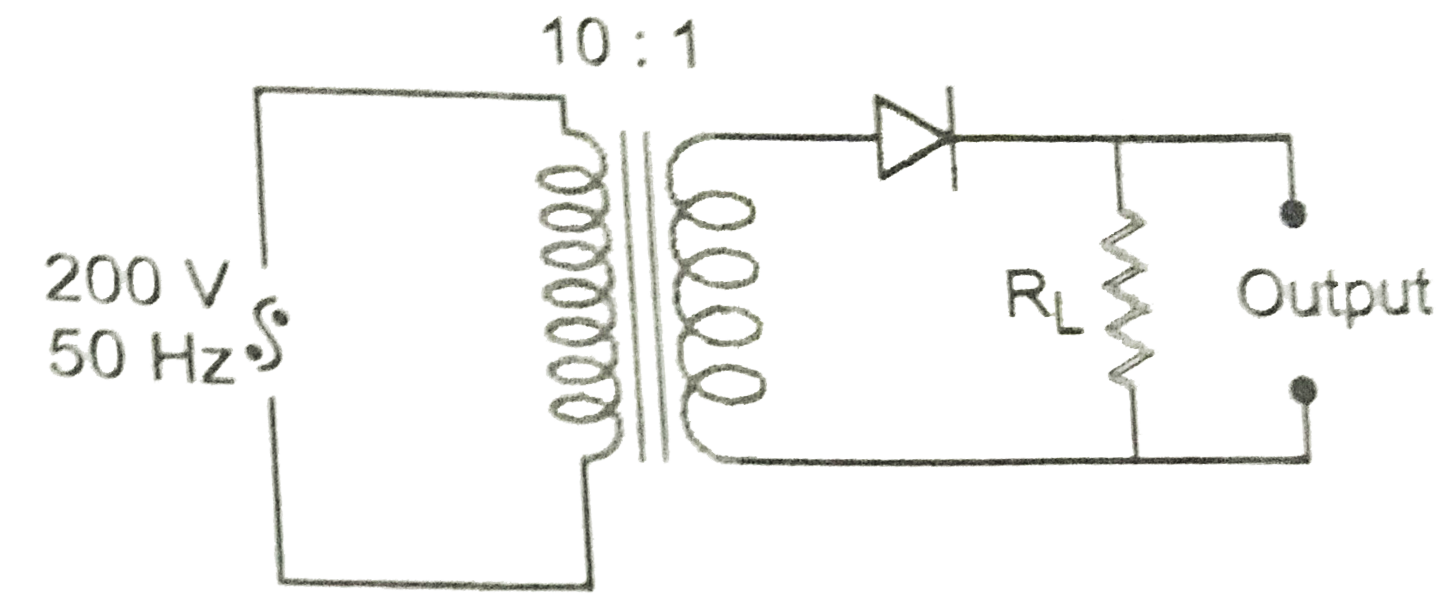 03:34View Solution
In a photo diode the conductivity increases when the material is exposed to light. It is found that the conductivity changes only if the wavelength of incident light is less than 500 nm. What is the band gap? Use `h=6.6xx10^(-34)Js, c=3xx10^(8) ms^(-1)`.
01:58View SolutionIn a silicon transistor, a change of `8.0 mA` in the emitter current produces a change of `7.9 mA` in the collector current. What change in the base current is necessary to produce an equivalent change in collector current?
02:04View SolutionThe current gain for common emitter amplifier is 69. If the emitter current is `7.0 mA`, find (i) base current and (ii) collector current.
02:20View SolutionThe potential difference across the collector of a transistor, used in common emitter mode is `1.5V`, with the collector resistance of `3 kOmega`. Find (i) the emitter current and (ii) the base current, if d.c. gain of the transistor is 50.
03:28View SolutionOutput characteristics of an n-p-n transistor in CE configuration is shown in the Fig. Determine
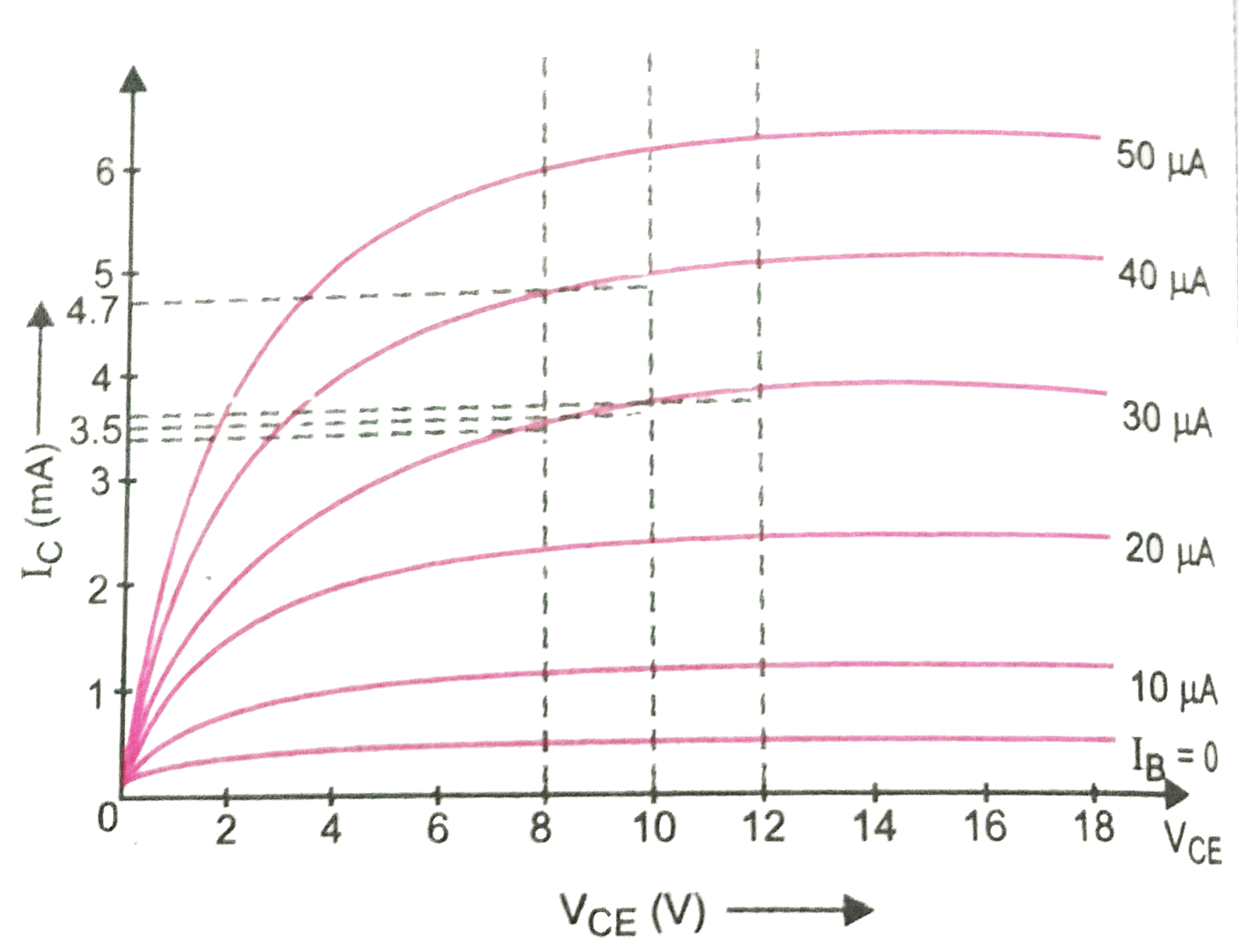
(i) dynamic output resistance (ii) dc current gain and (iii) ac current gain at an opererating point `V_(CE)=10V`, when `I_(B)=30muA`.04:44View SolutionThe base current of a transistor is 105 muA and collector current is `2.05mA`.
Determine the value of `beta, I_(e)` and `alpha`
A change of `27muA` in the base current produces a change of 0.65 mA in the collector current. Find `beta_(a.c.)`.03:56View SolutionIn a silicon transistor, base current is changed by `20muA`. This result in a change of `0.02V` in base-emitter voltage and a change of `2 mA` in the collector current.
Find the input resistance, `beta_(a.c.)` and transconductance of the transistor.
The transistor is used as an amplifier with the load resistance `5k Omega`. What is the voltage gain of the amplifier?03:32View SolutionThe input resistance of a silicon transistor is `665Omega`. Its base current is changed by `15 muA` which result in the change in collector current by `2mA`. This transistor is used as a common emitter amplifier with a load resistance of 5kOmega calculate current gain, `beta_(a.c.)`, transconductance `g_(m)` and voltage gain `A_(v)` of the amplifier.
04:22View SolutionA transistor, connected in common emitter configuration, has input resistance `R_(i)=2kOmega` and load resistance `6kOmega`. If `beta=60` and an input signal `10mV` is applied, calculate the (i) resistance gain, (ii) voltage gain (iii) the power gain and (iv) the value of the output signal.
02:21View SolutionA change of `0.2mA` in the base current cause a change of `5mA` in the collector current for a common emitter amplifier. (i) Find the a.c. current gain of the transistor (ii) If the input resistance is `2kOmega` and its voltage gain is 75. Calculate the load resistance used in the circuit.
03:19View SolutionA transistor is used in common-emitter mode in an amplifier circuit. It is found that when a signal of `20mV` is added to the base-emitter voltage, the base current changes by `20muA` and collector current changes by `1.5mA`. Determine the factor beta, input resistance `R_(i)`, the transconductance and voltage gain, Given load resistance `R_(L)=6kOmega`.
04:03View SolutionFor a common emitter transistor amplifier, the audio signal voltage across the collector resistance of `2kOmega` is 2V. If the current amplification factor of the transistor is 100, calculate (i) input signal voltage (ii) base current and (iii) power gain. Given that the value of the base resistance is `1kOmega`.
04:20View SolutionA full wave rectifier uses two diodes, the internal resistance of each diode may be assumed constant at `30 Omega`. The transformer r.m.s. secondary voltage from centre tap to each end of the secondary is 50 V and load resistance is `970 Omega`. Find (i) the mean load current (ii) the rms value of load current.
03:13View SolutionAn a.c. supply if `230V` is applied to a half wave rectifier circuit through a transformer of turn ratio 10:1. Find the output d.c. voltage. Assume the diode to be ideal.
04:19View SolutionA half wave rectifier is used to supply 50V d.c. to a resistance load of `800Omega`. Diode has a resistance of 200Omega. Calculate maximum a.c. voltage required.
03:02View SolutionIn a common emitter transistor amplifier, the input resistance of a transistor is `1000Omega`. On changing its base current by 10muA, the collector current increases by `2mA`. If a load resistance of `5kOmega` is used in the circuit, calculate:
(i) the currnet gain (ii)the voltage gain of the amplifier.03:45View SolutionA transistor is connected in common emitter configuration. The collector supply is 8V and the voltage drop across a resistor of `800Omega` in the collector circuit is 0.5 V. If the current gain factor `(alpha)` is 0.96, find the base current.
03:29View SolutionIn a full wave junction diode rectifier, the input a.c. has r.m.s. value of 20 V. The transformer used is a step up transformer having primary and secondary turns ratio 1: 2. Calculate the d.c. voltade in the recitified output.
04:15View SolutionIn a centre trap full wave rectifier, the load resistance `R_(L)=1kOmega`. Each diode has a forward bias dynamic resistance `20 Omega`. The voltage across half the secondary winding is 110 sin 100 pit. Find (i) the peak value of current (ii) the dc value of current (iii) the rms value of current.
02:55View SolutionFind the binary number of decimal number 42.
01:05View SolutionFind the decimal number of binary number `(111101.01)_(2)`
03:23View SolutionFind the binary number of `(23.50)_(10)`.
03:17View SolutionFind the equivalent binary number of decimal number `(9.25)_(10)`.
03:32View SolutionFind the binary (i) addition (ii) subtraction of the following set of numbers , 101010 and 010101.
06:29View SolutionThe truth table shown below in and belong to which gates?
(a) `|{:(A,B,Y),(0,0,0),(0,1,0),(1,0,0),(1,1,1):}|`
(b) `|{:(A,B,Y),(0,0,1),(1,0,1),(0,1,1),(1,1,0):}|`02:59View SolutionFind the output y of the logic gate whose symbol Is shown in Fig. and give a truth table for the same.
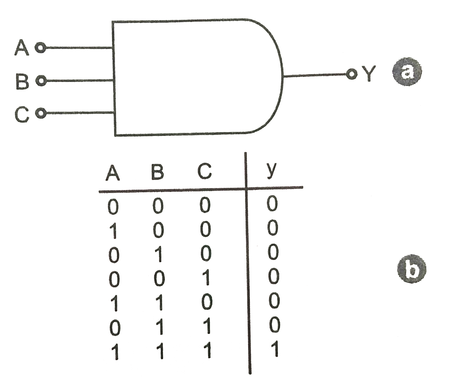 02:29View Solution
Find output y in the folowing circuit Fig.
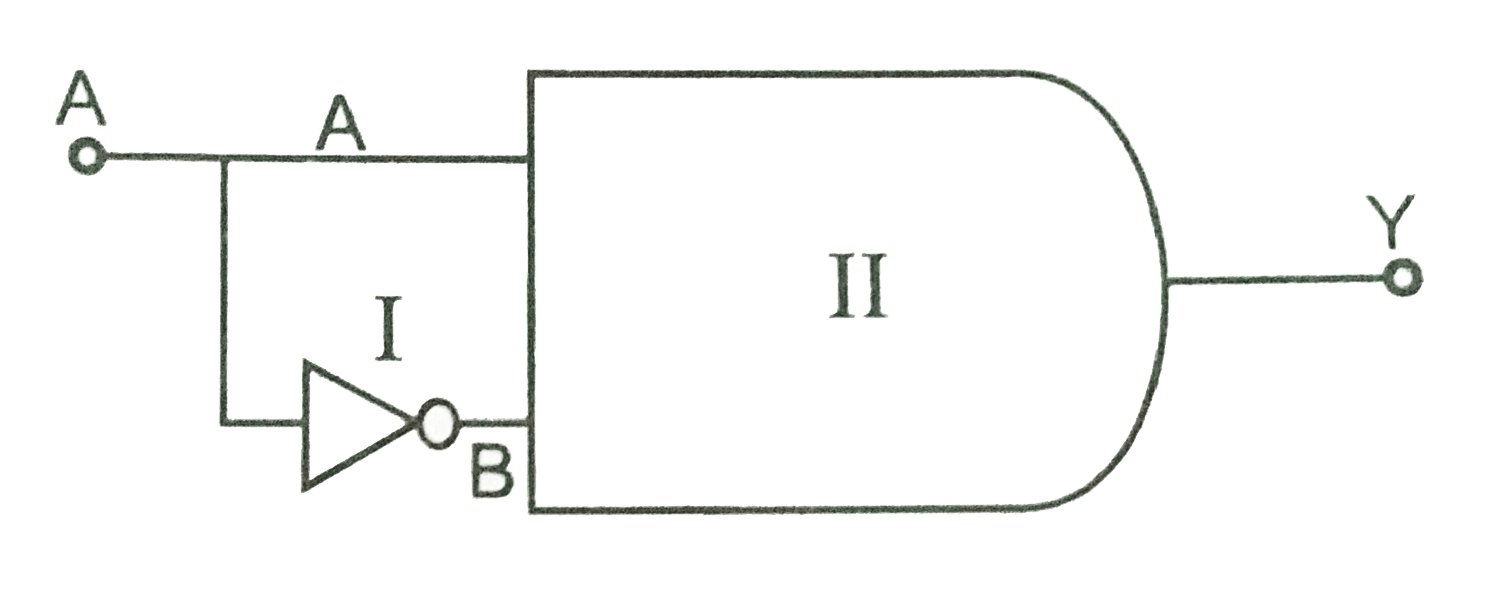 .01:14View Solution
Name the 2-input logic gate, whose truth table is given here, If this logic gate is connected to a NOT gate. What will be the output when
(i) `A=1, B=1` and (ii) `A=0, B=1`?
`|{:(A,B,"Output"y),(0,0,1),(0,1,1),(1,0,1),(1,1,0):}:|`
`|{:(A,B,"Out put"y,"Output of Not gate"),(1,1,0,1),(0,1,1,0):}|`02:56View Solution
Exercise questions and complete solutions for chapter ELECTRONIC DEVICES of PRADEEP PHYSICS (HINGLISH) of Class 12
All Exercises from PRADEEP Class 12 PHYSICS ELECTRONIC DEVICES
- ADVANCED PROBLEMS FOR COMPETITIONS
- CONCEPTUAL PROBLEMS
- Exercise
- EXERCISES (NCERT)
- Fill in the Blanks
- HIGHER ORDER THINKING SKILLS
- INTEGER TYPE QUESTION
- LONG QUESTION ANSWER
- LONG QUESTION ANSWER (NCERT)
- MCQ
- MULTIPLE CHOICE QUESTIONS
- PROBLEMS FOR PRACTICE
- SAMPLE PROBLEM
- SHORT QUESTION ANSWER
- Solved Examples
- VERY SHORT QUESTION ANSWER (NCERT)
