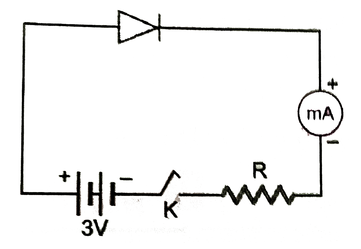
When a p-type semiconductor is brought into a close contact with n-type semiconductor, we get a p-n junction with a barrier potential 0.4V and the width of depletion region is 4.0×10⁻⁷m. this p-n junction is forwaed biased with a battery of voltage 3V adn negligible internal resistance, in series with a resistance of resistance R, ideal milliammeter with reading 20 mA and key K as shown in Fig.

The resistance of resistor R is
A
0.060 W
B
0.052 W
C
0.008 W
D
0.048 W
Video Solution
Text Solution
The correct Answer is:C
Wattage of diode = voltage drop across diode xx current
=0.4×20×10−3=0.008W
|
Updated on:21/07/2023
Related Playlists
- BOOK - PRADEEPCHAPTER - ELECTRONIC DEVICESEXERCISE - INTEGER TYPE QUESTION2videos
ELECTRONIC DEVICES
- BOOK - PRADEEPCHAPTER - ELECTRONIC DEVICESEXERCISE - MULTIPLE CHOICE QUESTIONS2videos
ELECTRONIC DEVICES
- BOOK - PRADEEPCHAPTER - ELECTRONIC DEVICESEXERCISE - PROBLEMS FOR PRACTICE7videos
ELECTRONIC DEVICES
- BOOK - PRADEEPCHAPTER - ELECTROMAGNETIC WAVESEXERCISE - II Focus multiple choice question5videos
ELECTROMAGNETIC WAVES
- BOOK - PRADEEPCHAPTER - ELECTROSTATICSEXERCISE - ASSERTION-REASON TYPE QUESTIONS2videos
ELECTROSTATICS
Similar Practice Problems
- Question 1 - Select One
When a p-type semiconductor is brought into a close contact with n-type semiconductor, we get a p-n junction with a barrier potential 0.4V and the width of depletion region is 4.0×10⁻⁷m. this p-n junction is forwaed biased with a battery of voltage 3V adn negligible internal resistance, in series with a resistance of resistance R, ideal milliammeter and key K as shown in Fig.

The resistance of resistor R isA150ΩB300ΩC130ΩD180Ω - Question 1 - Select One
When a p-type semiconductor is brought into a close contact with n-type semiconductor, we get a p-n junction with a barrier potential 0.4V and the width of depletion region is 4.0×10⁻⁷m. this p-n junction is forwaed biased with a battery of voltage 3V adn negligible internal resistance, in series with a resistance of resistance R, ideal milliammeter with reading 20 mA and key K as shown in Fig.

The resistance of resistor R isA0.060 WB0.052 WC0.008 WD0.048 W - Question 1 - Select One
When a p-type semiconductor is brought into a close contact with n-type semiconductor, we get a p-n junction with a barrier potential 0.4V and the width of depletion region is 4.0×10⁻⁷m. this p-n junction is forwaed biased with a battery of voltage 3V adn negligible internal resistance, in series with a resistance of resistance R, ideal milliammeter and key K as shown in Fig.

The intensity of the electric field in the depletion region when p-n junction is unbiased isA0.5×106Vm−1B1.0×106Vm−1C2.0×106Vm−1D1.5×106Vm−1 - Question 1 - Select One
When a p-type semiconductor is brought into a close contact with n-type semiconductor, we get a p-n junction with a barrier potential 0.4V and the width of depletion region is 4.0×10⁻⁷m. this p-n junction is forwaed biased with a battery of voltage 3V adn negligible internal resistance, in series with a resistance of resistance R, ideal milliammeter with reading 20 mA and key K as shown in Fig.

The resistance of resistor R isA1.39×105ms−1B2.78×105ms−1C1.39×106ms−1D2.78×106ms−1 - Question 1 - Select One
When n and p-type semiconductors are allowed to come into contact
Asome electrons will flow from n to pBsome electrons will flow from p to nCthe impurity element will flow from n to pDthe impurity element will flow from p to n - Question 1 - Select One
In a p-n junction , the barrier potential offers resistance to
AFree electrons in n-side and holes in p-sideBfree electrons in p-side and holes in n-sideCOnly free electrons in n-sideDOnly holes in p-side - Question 1 - Select One
In P−N junction, the barrier potential offerse resistance to
AThe resistance of intrinsic of semiconductor decrease with increases of temperatureBDoping pure Si with interval impurities give P-type semiconductorCOnly free electrons in N -type semiconductor are holesDOnly holes in P region

