Complete Solutions to Exercise 1 ( TOPICAL PROBLEMS ) of chapter SEMICONDUCTORS of Class 12 book with complete answers and questions
| Class 12 | PHYSICS |
| Chapter | SEMICONDUCTORS |
| MHTCET PREP GUIDE | Exercise 1 ( TOPICAL PROBLEMS ) |
| Number Of Questions | 84 |
| Academic Year | 2023-24 |
When the conductivity of a semiconductor is only due to breaking of covalent bonds, the semi conductor is called.
02:24View SolutionIf a small amount of antimony is added to germanium crystal
02:44View SolutionThe maximum wavelength of electromagnetic radiation, which can create a hole-electron pair in germanium. (Given that forbidden energy gap in germanium is 0.72 eV)
01:59View SolutionBasic building blocks of all electronic circuits are
01:49View SolutionIn a crystal, atomic separation is around 2A to 3A. At this separation due to interatomic interaction, energies of
View SolutionGas is-
01:42View SolutionThere is no hole current in conductors because they have
01:33View SolutionIf `N_(P)` and `N_(e)` be the numbers of holes and conduction electrons in an extrinsic semiconductor, then
02:10View SolutionAn n-type and p-type silicon can be obtained by doping pure silicon with.
03:21View SolutionIn an insulator, the forbidden energy gap between the valence band and conduction band is of the order of
01:03View SolutionCorrect one is
03:00View SolutionForbidden energy gap in a semiconductor is
01:31View SolutionIn its crystalline structure, every Si or Ge atoms are attached to other atoms by
01:36View SolutionLet `n_(p) and n_(e)` be the number of holes and conduction electrons respectively in a semiconductor. Then,
02:17View SolutionAt elevated temperature, few of covalent bonds of Si or Ge are broken a vacancy in the bond is created. Effective charge of vacancy or hole is
01:36View SolutionCarbon, silicon and germanium atoms have four valence electrons each. Their valence and conduction bands are separated by energy band gaps represented by `(E_(g))_(C),(E_(g))_(Si)` and `(E_(g))_(Ge)`, respectively. Which one of the following relationship is true in their case?
01:51View SolutionA intrinsic semiconductor at a absolute zero of temperature behaves as
01:17View SolutionWould there be any advantage to adding `n`-type or `p`-type impurities to copper
03:49View SolutionThe temperature of germanium is decreased from room temperature to 100 K, the resistance of germanium
02:40View SolutionThe contribution in the total current flowing through a semiconductor due to electrons and holes are `3/4` and `1/4` respectively. If the drift velocity of electrons is `5/2` times that of holes at this temperature, then the ratio of concentration of electrons and holes is
03:28View SolutionWhich one of the following statements is false ?
03:33View SolutionThe forward biased diode connection is
01:53View SolutionReverse bias applied to a junction diode
02:04View SolutionIn a reverse biased p-n junction, when the applied bias voltages is equal to the breakdown voltage, then
03:51View SolutionIn a p- n junction diode not connected to any circuit,
03:07View SolutionWhen LED is forward biased, then
04:17View SolutionA full wave rectifier uses two diodes with a load resistance of `100 Omega`. Each diode is having negligible forward resistance. Find the efficiency of this wave rectifier.
01:34View SolutionIn forward biasing of the p-n junction:
01:39View SolutionIn a `P-N` junction diode :
03:41View SolutionIn the middle of the depletion layer of a reverse - biased `p - n ` junction , the
04:48View SolutionIn a semi conductor diode , the barrier potential offers opposition to only -
01:33View SolutionFor germenium crystal, the forbidden energy gap in joules is
01:13View SolutionA 220 V AC supply is connected between points A and B.
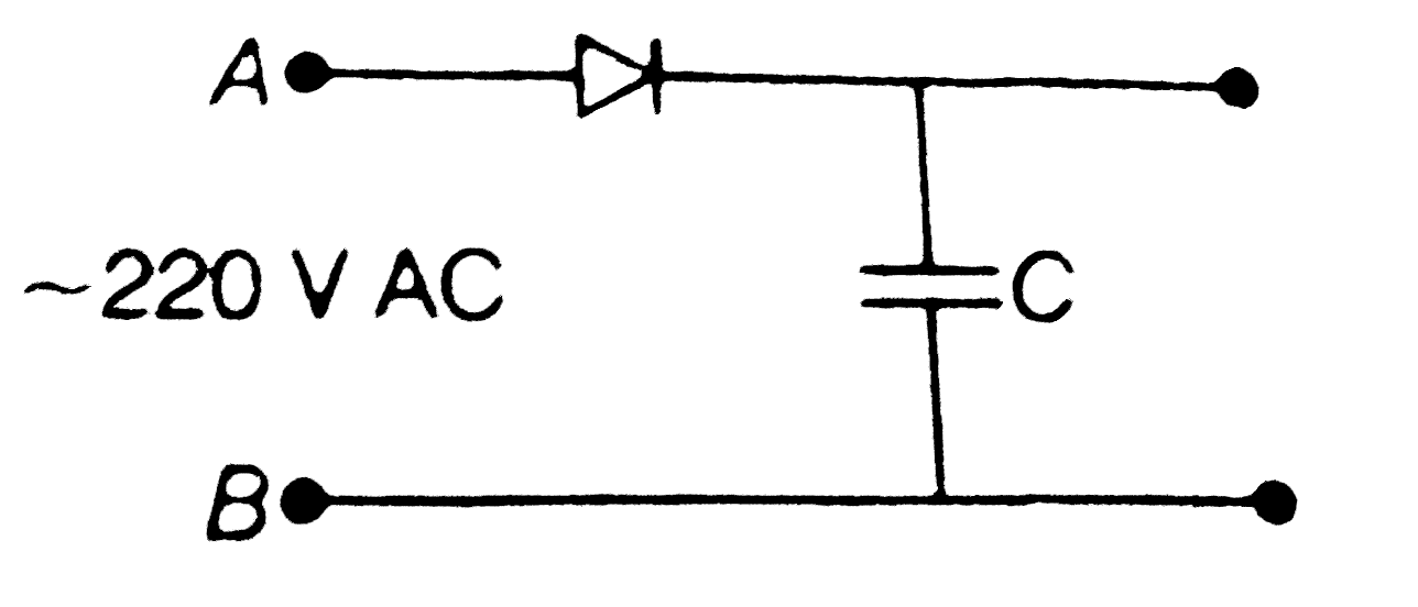
What will be potential difference across capacitor C ?03:39View SolutionIf an alternating voltage is applied across a diode in series with a load, then
02:57View SolutionIn half - wave rectification, what is the output frequency, if the input frequency is 50 Hz ? What is the output frequency of a full - wave rectifier for the same input frequency ?
03:06View SolutionThe p-n junction which generates an emf when solar radiation falls on it, with no external bias applied, is a
03:19View SolutionAvalanche breakdown in a `PN` junction diode is to
05:57View SolutionIf in a `p-n ` junction diode , a square input single of `10 V` is applied as shown
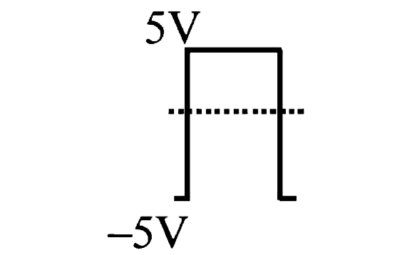
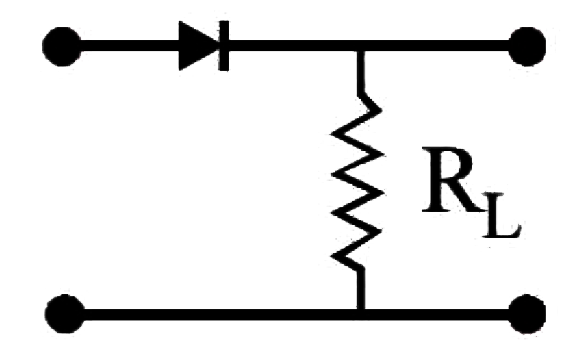 01:36View Solution
Pure Si at 300 K has equal electron `(n_(e))` and hole `(n_(h))` concentrations of `1.5xx10^(16)m^(-3)` doping by indium increases `n_(h)` to `4.5xx10^(22)m^(-3)`. Caculate `n_(e)` in the doped Si-
01:20View SolutionIn an unbiased p-n junction,
02:15View SolutionThe difference in the variation of resistance with temperature in a metal and a semiconductor arises essentially due to the difference in the
02:33View SolutionIn semiconductor the concentrations of electron and holes are `8xx10^(18)//m^(3)` and `5xx10^(18)//m` respectively. If the mobilities of electrons and hole are `2.3 m^(2)//`volt-sec and `0.01m^(2)//` volt-sec respectively, then semicondutor is
02:58View SolutionA light emitting diode `(LED)` has a voltage drop of `2V` across it and passes a current of `10 mA`. When it operates with a `6V` battery through a limiting resistor `R`. The value of `R` is
01:32View SolutionRectifier converts
02:09View SolutionThe probability of electrons to be found in the conduction band of an intrinsic semiconductor at a finite temperature
02:24View SolutionA transistor is operated in common emitter configuration at `V_(c)=2 V` such that a change in the base current from `100 muA` to `300 muA` produces a change in the collector current from `10 mA` to `20 mA`. The current gain is
02:07View SolutionAn n-p-n transistor can be considered to be equivalent to two diodes, connected. Which of the following figures is the correct one ?
03:32View SolutionThe transfer characteristics of a base biased transistor has the operation regions, namely, cutoff, active region and saturation region. For using the transistor as an amplifier it has to operate in the
01:24View SolutionFor a transistor the parameter `beta=99`. The value of the parameter `alpha` is
01:08View SolutionThe current gain in the common emitter mode of a transistor is 10. The input impedance is `20kOmega` and load of resistance is `100k Omega`. The power gain is
01:52View SolutionIf `beta, R_(L)` and r are the AC current gain, load resistance and the input resistance of a transistor respectively in CE configuration, the voltage and the power gains respectively are
02:03View SolutionIn a common base configuration (transistor circuit) `I_(E)=1mA, I_(C)=0.95mA`. The value of base current is
01:42View SolutionIn case of `NPN`-transistor the collector current is always less than the emitter current because
02:39View SolutionThe input resistance of a common emitter transistor amplifier, if the output resistance is `500 kOmega`, the current gain `alpha=0.98` and the power gain is `6.0625 xx 10^(6)` is
01:47View SolutionAn amplifier has a voltage gain `A_(v)= 1000`. The voltage gain in `dB` is:
01:02View SolutionA `p-n-p` transistor is said to be in active region of operation, When
02:00View SolutionThe current of transistor in common emitter mode is 49. The change in collector current and emitter current corresponding to the change in the base current by `5.0 muA`m will be :-
01:50View SolutionA transistor can be used practically in
01:18View SolutionIn an n-p-n transistor in CE configuration when `V_(BE)` is increased by small amount, then
01:12View SolutionFor a transistor circuit, `I_(B)=10mA` and `I_(C)=5.2mA`,
07:18View SolutionThe current gain of a common base transistor circuit is 0.96. On changing the emitter current by 10.0 mA, the change in the base current will be
01:51View SolutionIn case of `NPN`-transistor the collector current is always less than the emitter current because
02:39View SolutionIn transistor, forward bias is always smaller than the reverse bias. The correct reason is
02:43View SolutionThe device that can act as a complete electronic circuit is
02:18View SolutionThe voltage gain of an amplifier with `9%` negative feedback is `10`. The voltage gain without feedback will be
01:59View SolutionThe minimum potential difference between the base and emitter required to switch a silicon transistor ON is approximately?
01:15View SolutionIn the `CB` mode of a transistor, when the collector voltage is changed by `0.5` volt. The collector current changes by `0.05 mA`. The output resistance will be
02:12View SolutionSymbolic representation of four logic gates are shown as
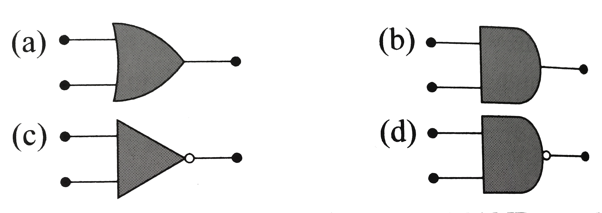 01:43View Solution
Symbolic representation of NOR gate is
01:12View SolutionThe output of given logic circuit is
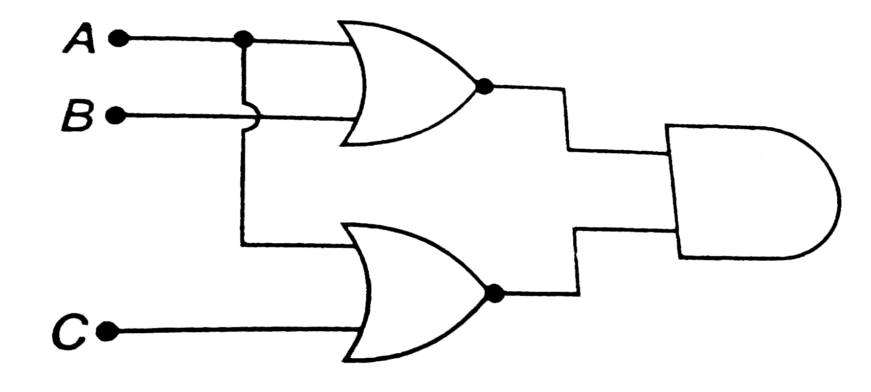 01:38View Solution
To get an output 1 from the circuit shown in the figure, the input must be
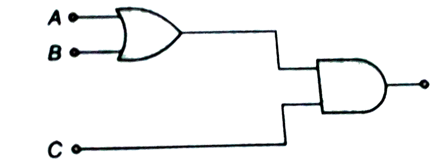 01:27View Solution
The circuit is equivalent to
 02:08View Solution
The output y, when all three inputs are first high and then low, will respectively be02:16View SolutionAn `AND` gate is following by a `NOT` gate in series. With two inputs `A` & `B`, the Boolean expression for the out put `Y` will be :
01:31View SolutionWhich logic gate is represented by the following combination of logic gates
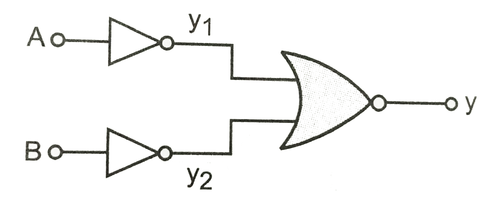 03:09View Solution
To which logic gate does the truth table given below correspond ?
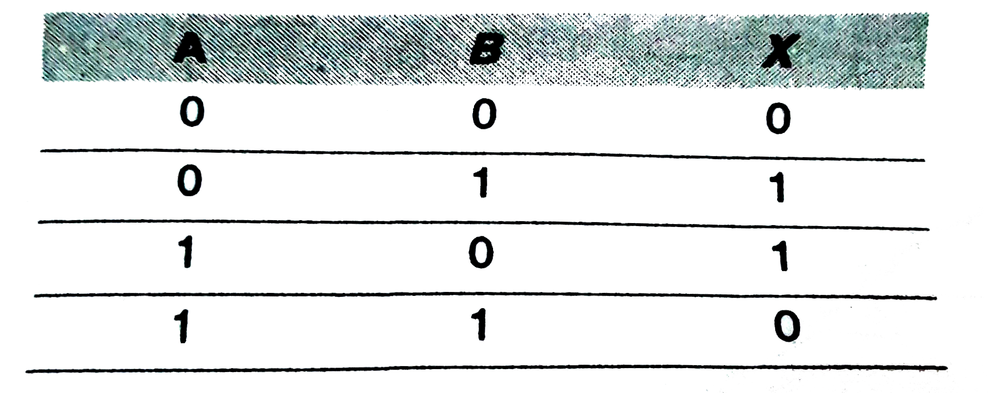 02:50View Solution
In Boolean algebra `A + B = Y` implies that :
01:59View SolutionDigital circuit can be made by repetitive use of
02:11View SolutionIf `A = B = 1`, then in terms of Boolean algebra the value of `A.B + A` is not equal to.
01:37View SolutionFor the given combination of gates, if the logic states of inputs `A,B,C,` are as follows `A=B=C=0` and `A=B=1, C=0` then the logic states of output `D` are
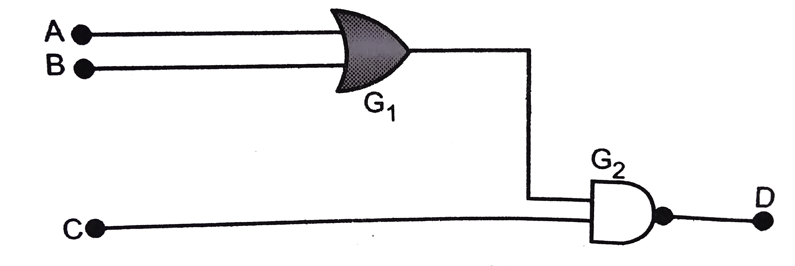 02:46View Solution
Which of the following gates will have an output of 1
01:50View SolutionWhat will be the input of `A` and `B` for the Boolean expression `bar((A+B)).bar((A.B))=1`?
02:26View SolutionTo get an output 1 from the circuit shown in the figure, the input must be
 01:27View Solution
Which of the following is the truth table for the circuit below ?
 01:46View Solution
Exercise 1 ( TOPICAL PROBLEMS ) questions and complete solutions for chapter SEMICONDUCTORS of MHTCET PREVIOUS YEAR PAPERS AND PRACTICE PAPERS of Class 12
