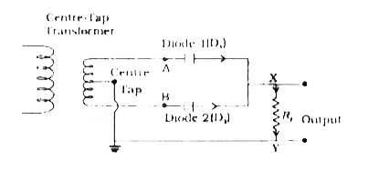
(a) A student wants to use tow p-n junction diodes to convert alternating current in to direct curent draw the labelled circuit diagram she would use and explain how it works
(b) give the truth table and circuit symbol for NAND gate
The labeled circuit diagram ,for the required circuit is as shown

The working of this circuits is as follows
(i) During one half cycle (of the input ac) diode D1 alone gets forward biased and conducts. During the other half cycle. it is aodel D2 (alone ) that conducts.
Because of the use of the center tapped transformer the current though the lead flows in the same direction in both the half cycles. Hence we get a unidirectional /direct current through the load , when the input as altermating current [Altermatively : The student may just use the following diagrams to explain the working.]
(##DBTSMPHYXIIDL18_E02026_S02##)
Topper's Solved these Questions
- 2018 QUESTION PAPER (DELHI ) BOOK - CBSE COMPLEMENTARY MATERIALCHAPTER - 2018 QUESTION PAPER (DELHI ) EXERCISE - SECTION E
15 Videos
- 2018 QUESTION PAPER (DELHI ) BOOK - CBSE COMPLEMENTARY MATERIALCHAPTER - 2018 QUESTION PAPER (DELHI ) EXERCISE - SECTION E
15 Videos
- CBSE BOARD EXAMNATION PAPER (2017 )BOOK - CBSE COMPLEMENTARY MATERIALCHAPTER - CBSE BOARD EXAMNATION PAPER (2017 )EXERCISE - SECTION E
12 Videos
Similar Questions
(a) A student wants to use tow p-n junction diodes to convert alternating current in to direct curent draw the labelled circuit diagram she would use and explain how it works
(b) give the truth table and circuit symbol for NAND gate
View SolutionDrawa labelled diagram of a full-wave rectifier circuit and briefly explain its working, Show the input-output waveforms.
Or
A student wants to use two p-n junction diodes to convert a.c. into d.c. Draw the labelled circuit diagram she would use and explain how it works.
View SolutionExplain the formation of depletion layer and potential barrier in p-n junction.
Draw the circuit diagram of a half wave rectifier and explain its working.
View SolutionDraw a labelled circuit diagram of a common base amplifier using a p-n-p transistor. Define the term voltage gain and write an expression for it.
View SolutionWhat is rectification? With the help of labelled circuit diagram explain half wave rectification using a junction diode.
View SolutionWhat is a p-n junction diode? Define the term 'dynamic resistance' for the junction diode. With the help of a circuit diagram explain the working of a p-n junction diode as a full wave rectifier.
View SolutionWhat is rectification Draw relevant circuit diagram and waveforms explain the working of p-n jucntion diode as a full wave rectifier
View SolutionExplain with a neat diagram, how a p-n junction diode is used as a half wave rectifier.
View SolutionWith the help of circuit diagram explain, the working of p-n junction diode as half wave rectifier.
View SolutionExplain with the help of a circuit diagram, the working of a p−n junction diode as a half wave rectifier.
View Solution
