Assertion: The logic gate NOT can be built using diode.
Reason: The output voltage and the input voltage of the diode have 180∘ phase difference.
If both the assertion and reason are true and reason is a true explantion of the assertion.
If both the assertion and reason are true but the reason is not true the correct explantion of the assertion.
If the assertion is true but reason false
If both the assertion and reason are false.
The correct Answer is:D
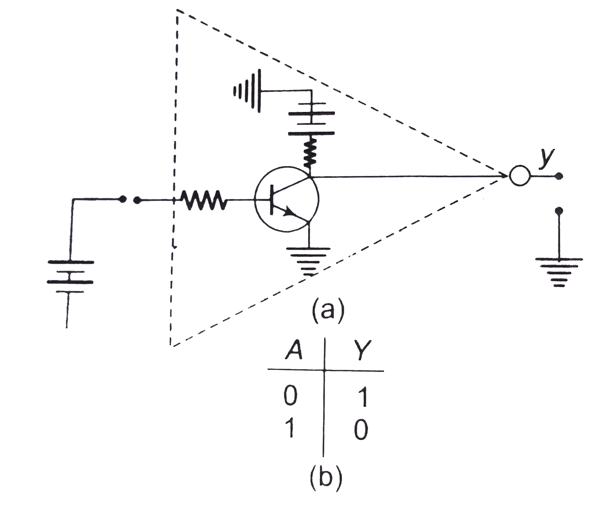
The NOT gate has only one input and one output. It combines the input A with the output Y, from Boolean expression
¯¯¯A=Y
We cannot realise a NOT gate by using diodes.

Instead a transistor has to be used. An electric circuit and truth table for a NOT gate using a n−p−n transistor is shown.
Topper's Solved these Questions
- SEMICONDUCTOR ELECTRONICSBOOK - A2ZCHAPTER - SEMICONDUCTOR ELECTRONICSEXERCISE - SECTION -D
1 Videos
- SEMICONDUCTOR ELECTRONICSBOOK - A2ZCHAPTER - SEMICONDUCTOR ELECTRONICSEXERCISE - EXERCISE
29 Videos
- SEMICONDUCTOR ELECTRONICSBOOK - A2ZCHAPTER - SEMICONDUCTOR ELECTRONICSEXERCISE - AIIMS Questions
38 Videos
- NUCLEAR PHYSICSBOOK - A2ZCHAPTER - NUCLEAR PHYSICSEXERCISE - Section D - Chapter End Test
29 Videos
- SOURCE AND EFFECT OF MAGNETIC FIELDBOOK - A2ZCHAPTER - SOURCE AND EFFECT OF MAGNETIC FIELDEXERCISE - Section D - Chapter End Test
30 Videos
Similar Questions
Assertion : In transistor, common emitter configuration is used to make a NOT gate.
Reason : In common emitter configuration, output voltage and input voltage have 180∘ phase difference.
View SolutionWhat is the phase relationship in the output and input voltage in the common base transistor amplifier.
View Solution
Knowledge Check
In a positive feedback oscillator, the feedback voltage (signal) and the input signal (voltage) have a phase difference of
A45∘B90∘C180∘D0∘In a voltage regulating of zener diode, the graph of output voltage vo versus input voltage v1 is
A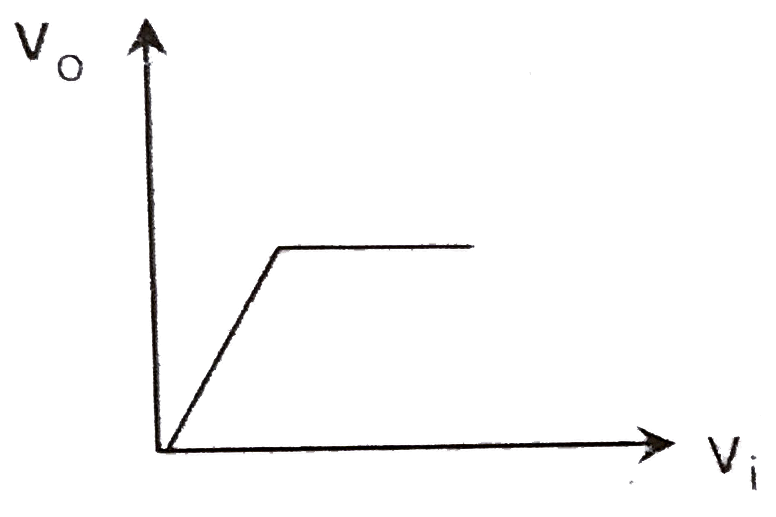 B
B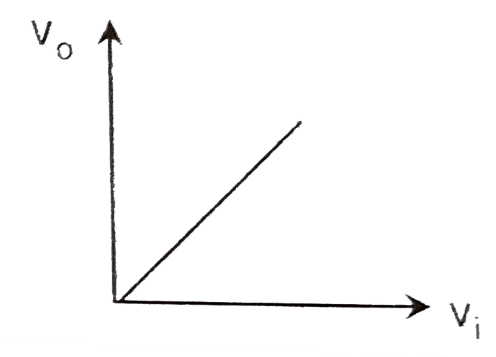 C
C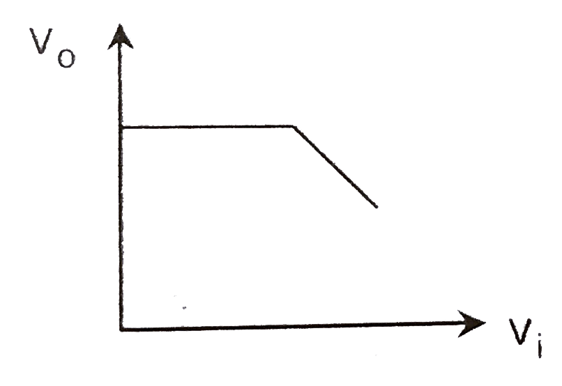 D
D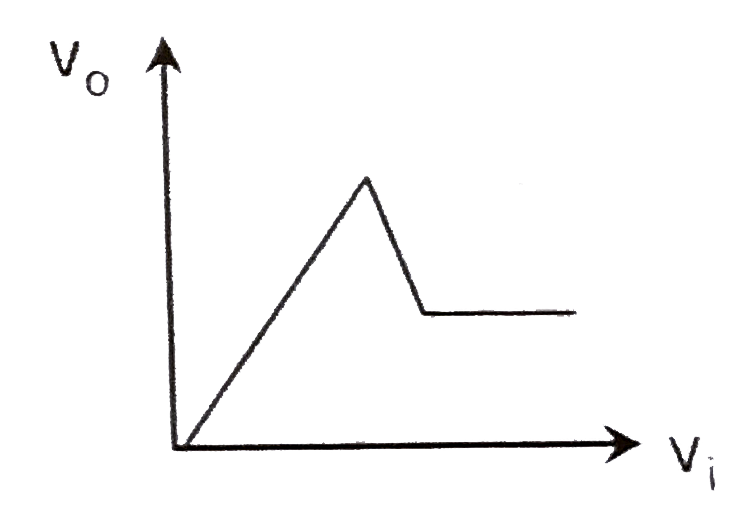
Assertion : Any logic can be constructed using NAND gate
Reason : NAND gate can be converted to OR gate by simply joining the two inputs.Aif both the Assertion and Reason are true and the Reason is the correct explanation of Assertion.Bif both the Assertion and Reason are true but the reason in not a correct explanation of the Assertion.Cif the Assertion is true but the Reason is false.Dif both Assertion and Reason are false.
The phase difference between input and output voltage of a CE circuit is
View SolutionIn a common-base amplifier, the phase difference between the input signal voltage and output voltage is :
View SolutionIn a common emitter amplifier, the phase difference between the input signal voltage and output voltage is.
View SolutionIn a common emitter amplifier, the input and output voltage are out of phase by
View SolutionAssertion: In a transistor amplifier, the output voltage is always out of phase with the input voltage.
Reason: The emitter base junction is reverse biased and the base collector junction is forward biased.
View Solution
