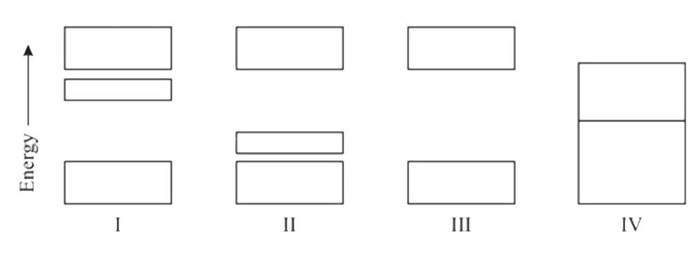
Define Fermi energy level. Represent Fermi level on band diagram for pure semiconductor, N-type and P-type semiconductor
Step-by-Step Solution
Step 1: Define Fermi Energy Level
The Fermi energy level, often referred to simply as the Fermi level, is defined as the highest energy level that an electron can occupy at absolute zero temperature (0 Kelvin). At this temperature, all the energy states below the Fermi level are filled with electrons, while those above it are empty.
Step 2: Understand the Types of Semiconductors
Semiconductors can be classified into two main types:
- Intrinsic (Pure) Semiconductors: These are pure forms of semiconductor materials without any significant dopant atoms present.
- Extrinsic (Doped) Semiconductors: These are semiconductors that have been intentionally doped with impurities to modify their electrical properties. They are further divided into:
- N-type Semiconductors: Doped with elements that have more valence electrons than the semiconductor (e.g., phosphorus in silicon), resulting in an abundance of electrons.
- P-type Semiconductors: Doped with elements that have fewer valence electrons than the semiconductor (e.g., boron in silicon), resulting in an abundance of holes.
Step 3: Represent Fermi Level on Band Diagram for Pure Semiconductor
In an intrinsic semiconductor, the Fermi level is positioned exactly in the middle of the conduction band and the valence band. This is because the number of electrons in the conduction band is equal to the number of holes in the valence band.
Diagram Representation:
ConductionBand⊢−−−−−−−−−−−−−−−−−FermiLevel−−−−−−−−−−−−−−−−−−−|∣|∣∣Va≤nceBand
Step 4: Represent Fermi Level on Band Diagram for P-type Semiconductor
In a P-type semiconductor, there are more holes in the valence band than there are electrons in the conduction band. Therefore, the Fermi level is closer to the valence band.
Diagram Representation:
ConductionBand⊢−−−−−−−−−−−−−−−−−FermiLevel−−−−−−−−−−−−−−−−−−−|||∣|||Va≤nceBand
*Note: The Fermi level is closer to the valence band in this diagram.*
Step 5: Represent Fermi Level on Band Diagram for N-type Semiconductor
In an N-type semiconductor, there are more electrons in the conduction band than there are holes in the valence band. Thus, the Fermi level is closer to the conduction band.
Diagram Representation:
ConductionBand⊢−−−−−−−−−−−−−−−−−FermiLevel−−−−−−−−−−−−−−−−−−−|||∣|||Va≤nceBand
*Note: The Fermi level is closer to the conduction band in this diagram.*
Summary
- The Fermi level is the highest energy level occupied by electrons at absolute zero.
- In intrinsic semiconductors, the Fermi level is in the middle of the band gap.
- In P-type semiconductors, the Fermi level is closer to the valence band.
- In N-type semiconductors, the Fermi level is closer to the conduction band.
The Fermi energy level, often referred to simply as the Fermi level, is defined as the highest energy level that an electron can occupy at absolute zero temperature (0 Kelvin). At this temperature, all the energy states below the Fermi level are filled with electrons, while those above it are empty.
Semiconductors can be classified into two main types:
- Intrinsic (Pure) Semiconductors: These are pure forms of semiconductor materials without any significant dopant atoms present.
- Extrinsic (Doped) Semiconductors: These are semiconductors that have been intentionally doped with impurities to modify their electrical properties. They are further divided into:
- N-type Semiconductors: Doped with elements that have more valence electrons than the semiconductor (e.g., phosphorus in silicon), resulting in an abundance of electrons.
- P-type Semiconductors: Doped with elements that have fewer valence electrons than the semiconductor (e.g., boron in silicon), resulting in an abundance of holes.
In an intrinsic semiconductor, the Fermi level is positioned exactly in the middle of the conduction band and the valence band. This is because the number of electrons in the conduction band is equal to the number of holes in the valence band.
ConductionBand⊢−−−−−−−−−−−−−−−−−FermiLevel−−−−−−−−−−−−−−−−−−−|∣|∣∣Va≤nceBand
In a P-type semiconductor, there are more holes in the valence band than there are electrons in the conduction band. Therefore, the Fermi level is closer to the valence band.
ConductionBand⊢−−−−−−−−−−−−−−−−−FermiLevel−−−−−−−−−−−−−−−−−−−|||∣|||Va≤nceBand
*Note: The Fermi level is closer to the valence band in this diagram.*
In an N-type semiconductor, there are more electrons in the conduction band than there are holes in the valence band. Thus, the Fermi level is closer to the conduction band.
ConductionBand⊢−−−−−−−−−−−−−−−−−FermiLevel−−−−−−−−−−−−−−−−−−−|||∣|||Va≤nceBand
*Note: The Fermi level is closer to the conduction band in this diagram.*
- The Fermi level is the highest energy level occupied by electrons at absolute zero.
- In intrinsic semiconductors, the Fermi level is in the middle of the band gap.
- In P-type semiconductors, the Fermi level is closer to the valence band.
- In N-type semiconductors, the Fermi level is closer to the conduction band.
Topper's Solved these Questions
- SEMICONDUCTOR DEVICESBOOK - AAKASH SERIESCHAPTER - SEMICONDUCTOR DEVICESEXERCISE - Exercise (very Short answer questions)
36 Videos
- SEMICONDUCTOR DEVICESBOOK - AAKASH SERIESCHAPTER - SEMICONDUCTOR DEVICESEXERCISE - Problems (LEVEL-I)
35 Videos
- SEMICONDUCTOR DEVICESBOOK - AAKASH SERIESCHAPTER - SEMICONDUCTOR DEVICESEXERCISE - Exercise (Long answer questions)
6 Videos
- RAY OPTICSBOOK - AAKASH SERIESCHAPTER - RAY OPTICSEXERCISE - PROBLEMS ( LEVEL-II)
60 Videos
- UNITS AND MEASUREMENTBOOK - AAKASH SERIESCHAPTER - UNITS AND MEASUREMENTEXERCISE - PRACTICE EXERCISE
45 Videos
Similar Questions
n-type semiconductor is
View SolutionA p-type semiconductor is
View SolutionA N - type semiconductor is
View SolutionWhat are n-type and p-type semiconductors?
View SolutionWhat are p-type and n-type semiconductors?
View SolutionWhat are n-type semiconductors ?
View SolutionThe band structure in n - type semiconductor is

View SolutionA 0K temperature, a p-type semiconductor
View SolutionDraw energy band diagram of conductors, semiconductors and insulators.
View SolutionWhat is a semiconductor ? Describe the two main types of semiconductors.
View Solution
