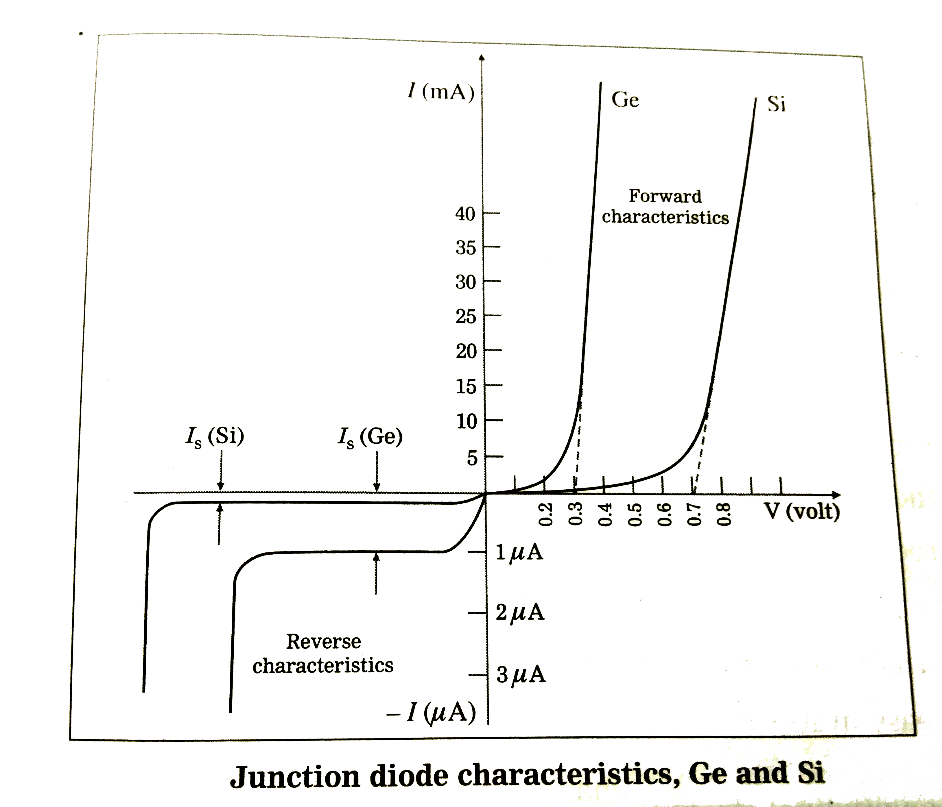
Draw the I - V characteristics of Ge and Si pn- junction diodes and explain the same .
Text Solution

Junction diode characteristics, Ge and Si
Explanation :
(1) Forward bias characteristics : There is forward current only after the barrier potential of the pn-junction is overcome. Then there is an exponential rise in the current beyond the knee region. The forward - bias voltage required to reach the region of upward swing is called the threshold voltage VT or cut in voltage. When rounded off to the nearest , the threshold voltage is 0.3 V for a germanium diode and 0.7 V for a silicon diode.
(2) Reverse bias characteristics : In the reverse bias, the potential barrier at the junction is large and the current due to majority carriers in each region is zero. However, minority charge carriers are able to cross the junction and constitute a very small current in the reverse direction. This reverse current quickly reaches its maximum or saturation value and remains fairly constant with increase in the reverse - bias voltage. It is called the reverse saturation current Is,
which is typically a few nanoamperes for a silicon diode and a few microamperes for a germanium diode.
Too high a negative voltage results in a sharp change in the reverse - bias characteristics. At a certain characteristic negative voltage, called the peak inverse voltage (PIV) or breakdown voltage, the current in the reverse direction increases very rapidly . In general, a silicon diode has a higher PIV rating (~1000V) than a germanium diode (~400V).
|
Updated on:21/07/2023
Topper's Solved these Questions
- BOOK - NAVNEET PUBLICATION - MAHARASHTRA BOARDCHAPTER - MODEL QUESTION PAPER EXERCISE - SECTION- D5videos
MODEL QUESTION PAPER
- BOOK - NAVNEET PUBLICATION - MAHARASHTRA BOARDCHAPTER - MODEL QUESTION PAPER EXERCISE - SECTION- B12videos
MODEL QUESTION PAPER
- BOOK - NAVNEET PUBLICATION - MAHARASHTRA BOARDCHAPTER - LAWS AND THEORIESEXERCISE - Assignments2videos
LAWS AND THEORIES
- BOOK - NAVNEET PUBLICATION - MAHARASHTRA BOARDCHAPTER - MODEL QUESTION PAPER FOR PRACTICEEXERCISE - SECTION-D5videos
MODEL QUESTION PAPER FOR PRACTICE
Similar Questions
Knowledge Check
- Question 1 - Select One
In a PN -junction diode
AThe current in the reverse biased condition is generally very smallBThe current in the reverse biased condition is small but the forwards biased current is independent of the biase voltageCThe reverse biased current is srongly dependent on the applied biase voltage.DThe forward biased current is very small in comparision to reverse biased current. - Question 2 - Select One
The PN junction diode is used as
AAn amplifierBA rectifierCAn oscilatorDA modulator - Question 3 - Select One
A PN junction diode cannot be used
Aas rectifierBfor converting light energy to electric energyCfor gettting light radiationDboth majority and minority carriers on either side of junction
Explain briefly, with the help of circuit diagram , how V-I characteristics of a p-n junction diode are obtained in (i) forward bias, and (ii) reverse bias. Draw the shapes of the characteristic curves obtained.
Or
Explain briefly, with the help of necessary diagrams, the forward and the reverse biasing of a p-n junction diode. Also draw their characteristic curves in the two cases.View SolutionI-V Characterstics Of Junction Diode|Questions
View SolutionA PN junction diode cannot be used
View SolutionIn revers bias pn-junction diode depletion layer width
View SolutionThe reverse biasing in a PN junction diode
View Solution
