If no external voltage is applied across P−N junction, there would be
No electric field across the junction
An electric field pointing from N -type to P -type side across the junction
An electric field pointing from P -type to N -type side across the junction
A temporary electric field during formation of P - N junction that would subsequently disappear
The correct Answer is:B
Step by step video, text & image solution for If no external voltage is applied across P-N junction, there would be by Physics experts to help you in doubts & scoring excellent marks in Class 12 exams.
Updated on:21/07/2023Topper's Solved these Questions
- ELECTRONICSBOOK - ERRORLESS CHAPTER - ELECTRONICSEXERCISE - Digital Electronics
2 Videos
- ELECTRONICSBOOK - ERRORLESS CHAPTER - ELECTRONICSEXERCISE - Valve Electronics (Diode and Triode)
3 Videos
- ELECTRON, PHOTON, PHOTOELECTRIC EFFECT AND X-RAYSBOOK - ERRORLESS CHAPTER - ELECTRON, PHOTON, PHOTOELECTRIC EFFECT AND X-RAYSEXERCISE - Self Evaluation Test
3 Videos
- ELECTROSTATICS BOOK - ERRORLESS CHAPTER - ELECTROSTATICS EXERCISE - Ordinary Thinking Objective Questions (Electric Flux and Gauss.s Law)
28 Videos
Similar Questions
Knowledge Check
The P-N junction is-
AAn ohmic resistanceBNon ohmic resistanceCA positive resistanceDA negative resistanceNo biase is applied to a P−N junction, then the current
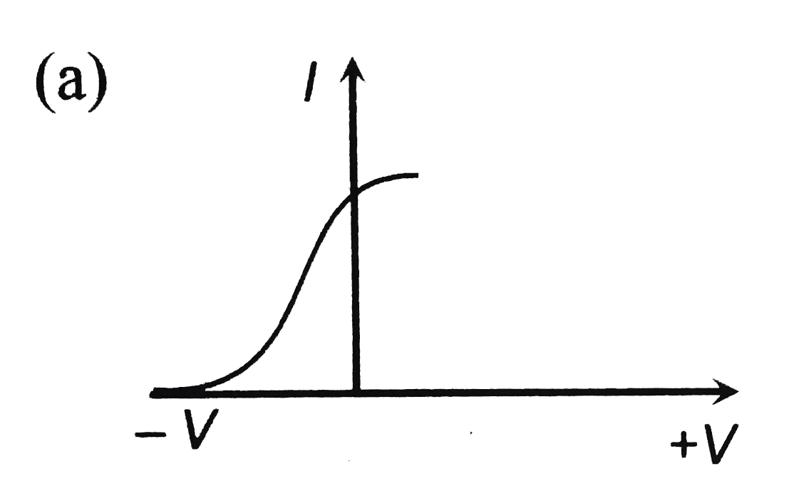
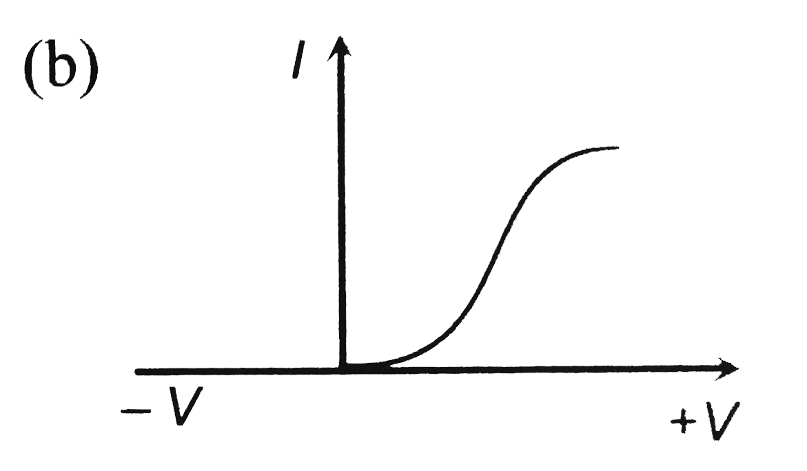
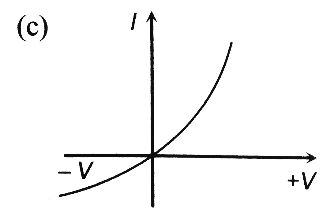
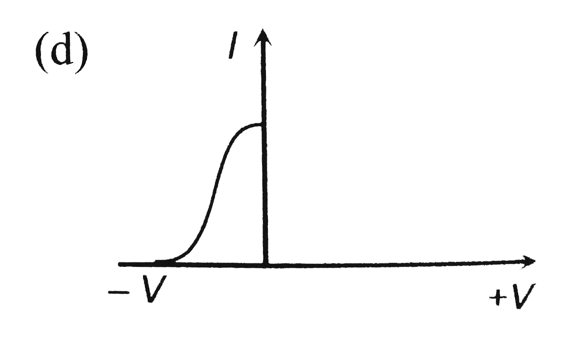
AIs zero because the number of charge carriers flowing on both sides is sameBIs zero because the charge carriers do not moveCIs non zeroDNone of theseDifferent voltages are applied across a P−N junction and the currents are measured for each value. Which of the following graphs is obtained between voltage and current?
A B
B C
C D
D
P-N junction diodes
View SolutionRead the following passage and then answer questions (a) - (e) on the basis of your understand- ing of the passage and the related studied concepts.
A semiconductor diode is basically a p-n junction and is thus a two terminal device, when an external voltage is applied across a semiconductor diode such that p-side is connected to the positive terminal of the battery and n-side to the negative terminal, it is forward biased. The direction of the applied voltage is opposite to the built in barrier potential. As a result, the depletion layer width decreases and the barrier height is reduced. If the applied voltage is increased, it may overcome the barrier potential altogether and a large current flows across the junction.
When an external voltage (V) is applied across the diode such that n-side is positive and p-side is negative, it is said to be reverse biased. The direction of applied voltage is same as the direction of barrier potential. As a result, the barrier height increases and the depletion region widens. So current flowing across the junction decreases enormously (practically becomes zero) as compared to the diode under forward bias.
If an alternating voltage is applied across a diode, the current flows only in that part of the cycle when the diode is forward biased.
Draw circuit arrangement of a p-n junction in forward bias and in revene bias arrangement.
View SolutionRead the following passage and then answer questions (a) - (e) on the basis of your understand- ing of the passage and the related studied concepts.
A semiconductor diode is basically a p-n junction and is thus a two terminal device, when an external voltage is applied across a semiconductor diode such that p-side is connected to the positive terminal of the battery and n-side to the negative terminal, it is forward biased. The direction of the applied voltage is opposite to the built in barrier potential. As a result, the depletion layer width decreases and the barrier height is reduced. If the applied voltage is increased, it may overcome the barrier potential altogether and a large current flows across the junction.
When an external voltage (V) is applied across the diode such that n-side is positive and p-side is negative, it is said to be reverse biased. The direction of applied voltage is same as the direction of barrier potential. As a result, the barrier height increases and the depletion region widens. So current flowing across the junction decreases enormously (practically becomes zero) as compared to the diode under forward bias.
If an alternating voltage is applied across a diode, the current flows only in that part of the cycle when the diode is forward biased.
Why is a p-n junction called semiconductor diode ?
View SolutionRead the following passage and then answer questions (a) - (e) on the basis of your understand- ing of the passage and the related studied concepts.
A semiconductor diode is basically a p-n junction and is thus a two terminal device, when an external voltage is applied across a semiconductor diode such that p-side is connected to the positive terminal of the battery and n-side to the negative terminal, it is forward biased. The direction of the applied voltage is opposite to the built in barrier potential. As a result, the depletion layer width decreases and the barrier height is reduced. If the applied voltage is increased, it may overcome the barrier potential altogether and a large current flows across the junction.
When an external voltage (V) is applied across the diode such that n-side is positive and p-side is negative, it is said to be reverse biased. The direction of applied voltage is same as the direction of barrier potential. As a result, the barrier height increases and the depletion region widens. So current flowing across the junction decreases enormously (practically becomes zero) as compared to the diode under forward bias.
If an alternating voltage is applied across a diode, the current flows only in that part of the cycle when the diode is forward biased.
Distinguish between forward bias and reverse bias arrangements of a semiconductor diode.
View SolutionRead the following passage and then answer questions (a) - (e) on the basis of your understand- ing of the passage and the related studied concepts.
A semiconductor diode is basically a p-n junction and is thus a two terminal device, when an external voltage is applied across a semiconductor diode such that p-side is connected to the positive terminal of the battery and n-side to the negative terminal, it is forward biased. The direction of the applied voltage is opposite to the built in barrier potential. As a result, the depletion layer width decreases and the barrier height is reduced. If the applied voltage is increased, it may overcome the barrier potential altogether and a large current flows across the junction.
When an external voltage (V) is applied across the diode such that n-side is positive and p-side is negative, it is said to be reverse biased. The direction of applied voltage is same as the direction of barrier potential. As a result, the barrier height increases and the depletion region widens. So current flowing across the junction decreases enormously (practically becomes zero) as compared to the diode under forward bias.
If an alternating voltage is applied across a diode, the current flows only in that part of the cycle when the diode is forward biased.
Name two main components of your mobile phone charger.
View Solution
