Increasing forward voltage in diode, the width of depletion layer is ……..Solution in Gujrati
decreases
increases
does not change
increases in proportion to the applied voltage
The correct Answer is:A
Step by step video, text & image solution for Increasing forward voltage in diode, the width of depletion layer is …….. by Physics experts to help you in doubts & scoring excellent marks in Class 12 exams.
Updated on:21/07/2023Topper's Solved these Questions
- SEMICONDUCTOR ELECTRONICS : MATERIALS, DEVICES AND SIMPLE CIRCUITS BOOK - KUMAR PRAKASHANCHAPTER - SEMICONDUCTOR ELECTRONICS : MATERIALS, DEVICES AND SIMPLE CIRCUITS EXERCISE - Section-D : Multiple Choice Questions (MCQs) (MCQs asked in Competitive Exams)
129 Videos
- SEMICONDUCTOR ELECTRONICS : MATERIALS, DEVICES AND SIMPLE CIRCUITS BOOK - KUMAR PRAKASHANCHAPTER - SEMICONDUCTOR ELECTRONICS : MATERIALS, DEVICES AND SIMPLE CIRCUITS EXERCISE - Section-C: NCERT Exemplar Solution (Long Answer Type Questions)
10 Videos
- SAMPLE QUESTION PAPER BOOK - KUMAR PRAKASHANCHAPTER - SAMPLE QUESTION PAPER EXERCISE - PART-B SECTION-C
5 Videos
- WAVE OPTICSBOOK - KUMAR PRAKASHANCHAPTER - WAVE OPTICSEXERCISE - SECTION-D (MULTIPLCE CHOICE QUESTIONS (MCQS)) (MCQS FROM DARPAN BASED ON TEXTBOOK)
239 Videos
Similar Questions
At absolute zero temperature Si acts as ……..
View Solution
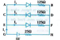
If each diode in figure has a forward bias resistance of 25Ω and infinite resistance in reverse bias, what will be the values of the current I1,I2,I3andI4?
View SolutionTwo charges –q and +q are located at points (0, 0, –a) and (0, 0, a), respectively.
(a) What is the electrostatic potential at the points (0, 0, z) and (x, y, 0) ?
(b) Obtain the dependence of potential on the distance r of a point from the origin when r/a>>1 .
(c) How much work is done in moving a small test charge from the point (5,0,0) to (–7,0,0) along the x-axis? Does the answer change if the path of the test charge between the same points is not along the x-axis?
View SolutionAccording to particle theory of light what is the velocity of light in a dense medium, compared to that in rare medium ?
View SolutionIf the forward voltage in a diode is increased, the width of the depletion region-
View Solutionअवक्षय परत की चौड़ाई पर क्या प्रभाव पड़ेगा यदि अग्र दिशिक विभव बढ़ा दी जाये ?
View SolutionIn forward bias the width of depletion layer is
View SolutionIf the forward voltage in p-n junction is increased , the length of depletion layer will
View SolutionThe knee voltage of a p-n junction diode is 0.8 V and the width of the depletion layer is 2muA . The electric field in the depletion layer is
View SolutionWhen reverse bias in a junction diode is increased, the width of depletion layer -
View SolutionIf the forward voltage in a semiconductor is doubled, the width of depletion layer will
View Solutionयदि क्रिस्टल डायोड का अग्र वोल्टेज बढ़ा दिया जाए, तो अवक्षय परत की मोटाई
View SolutionIf the forward voltage in a diode in increased, the width of the depletion region.
View SolutionIf the forward voltage in a diode is increased the width of the depletion region
View SolutionIf the forward voltage in a semiconductor is doubled, the width of depletion layer will
View Solution
