No biase is applied to a P−N junction, then the current
Is zero because the number of charge carriers flowing on both sides is same
Is zero because the charge carriers do not move
Is non-zero
None of these
The correct Answer is:B
Step by step video, text & image solution for No biase is applied to a P-N junction, then the current by Physics experts to help you in doubts & scoring excellent marks in Class 12 exams.
Updated on:21/07/2023Topper's Solved these Questions
- ELECTRONICSBOOK - ERRORLESS CHAPTER - ELECTRONICSEXERCISE - Digital Electronics
2 Videos
- ELECTRONICSBOOK - ERRORLESS CHAPTER - ELECTRONICSEXERCISE - Valve Electronics (Diode and Triode)
3 Videos
- ELECTRON, PHOTON, PHOTOELECTRIC EFFECT AND X-RAYSBOOK - ERRORLESS CHAPTER - ELECTRON, PHOTON, PHOTOELECTRIC EFFECT AND X-RAYSEXERCISE - Self Evaluation Test
3 Videos
- ELECTROSTATICS BOOK - ERRORLESS CHAPTER - ELECTROSTATICS EXERCISE - Ordinary Thinking Objective Questions (Electric Flux and Gauss.s Law)
28 Videos
Similar Questions
Explain with the help of a diagram, how depletion region and potential barrier are formed in a junction diode.
If a small voltage is applied to a p-n junction diode how will the barrier potential be affected when it is (i) forward biased and (ii) reverse biased?
View SolutionName the type of biasing of a p-n junction diode so that the junction offers very high resistance.
View Solution
Knowledge Check
No bias is applied to a P-N junction, then the current-
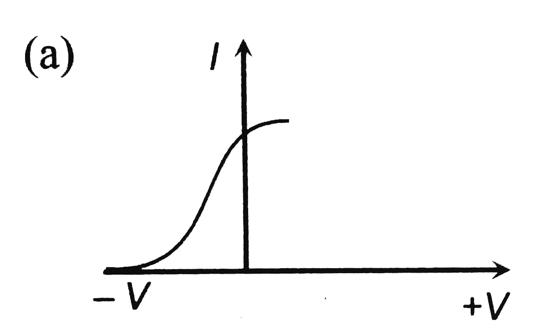
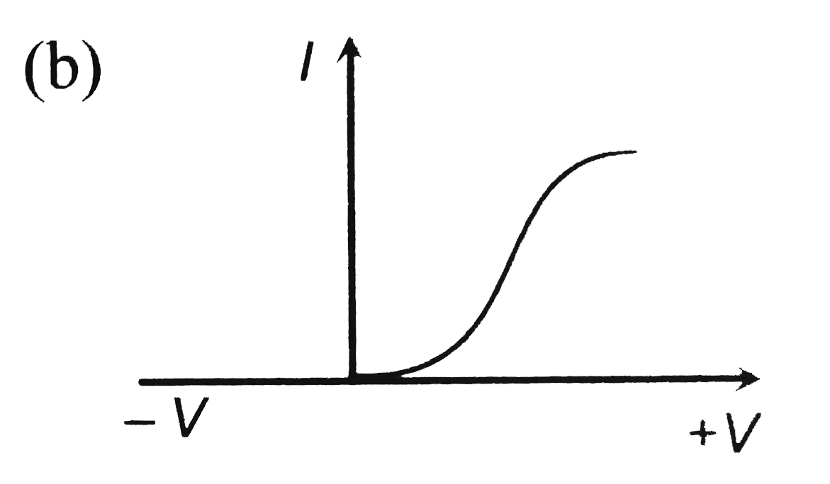
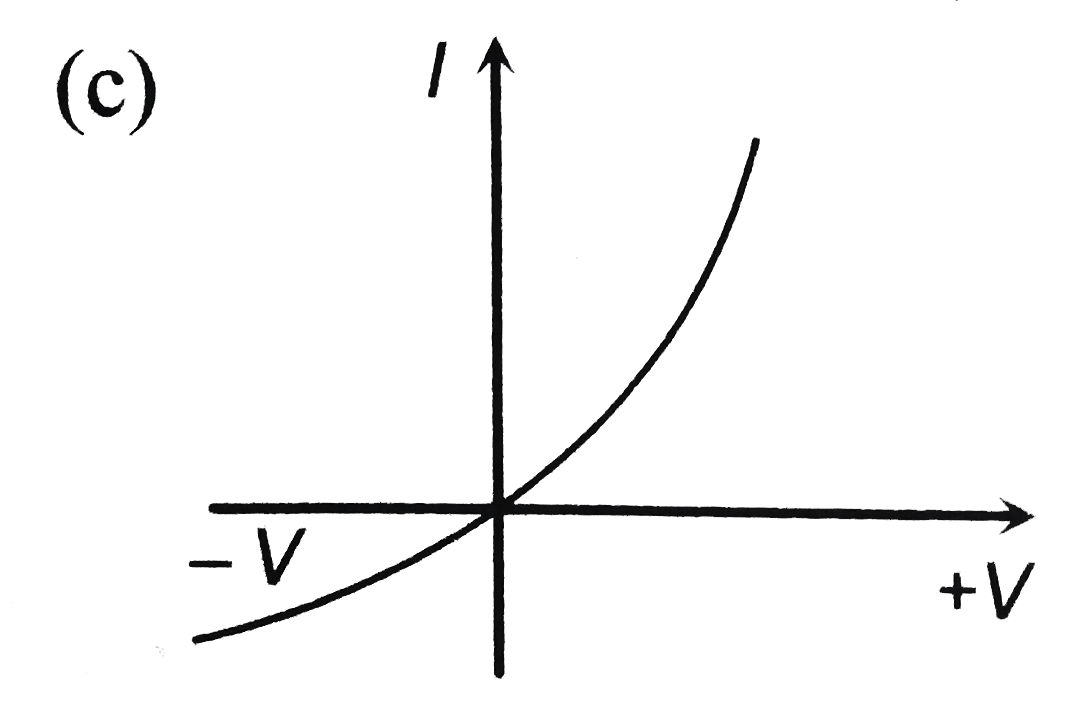
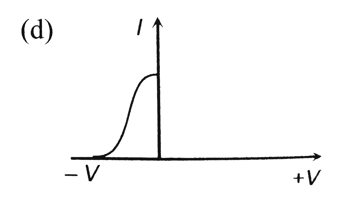
AIs zero because the number of charge carriers flowing on both sides is sameBis zero because the charge carriers do not moveCIs non-zeroDNone of theseDifferent voltages are applied across a P−N junction and the currents are measured for each value. Which of the following graphs is obtained between voltage and current?
A B
B C
C D
D
When a forward bias is applied to a p-n junction, it
Araises the potential barrier.Breduces the majority carrier current to zero.Clowers the potential barrier.Dnone of the above.
When a forward bias is applied to a p -n junction. It
View SolutionA potential difference is applied across (i) an issulator at 0 k (ii) a semiconductor at 0 k (iii) a metal at 0 k (iv) a reverse biased p-n junction diode at 300 k then the current passing through
View SolutionOn increases the reverse biase to a large value of in a PN- junction diode, current.
View SolutionAssertion:The dominant mechanism for motion of charge carriers in forward and reverse biased silicon P−N junction are drift in both forward and reverse biase.
Reason: In reverse biasing, no current flow through the junction.
View SolutionAssertion : The dominant mechanism for motion of charge carreis in forward and reverse biased silicon P-N junction are drit in both forward and reverse bias.
Reaon : In reverse biasing, no current flow through the junction.
View Solution
