Complete Solutions to EXERCISE -2 (H.W) (JUNCTION DIODES) of chapter SEMICONDUCTOR ELECTRONICS of Class 12 book with complete answers and questions
| Class 12 | PHYSICS |
| Chapter | SEMICONDUCTOR ELECTRONICS |
| NARAYANA | EXERCISE -2 (H.W) (JUNCTION DIODES) |
| Number Of Questions | 5 |
| Academic Year | 2023-24 |
The width of depletion region in p-n junction diode is `500 nm` and an intrinsic electric field of `6xx 10^(5) Vm^(-1)` is also found to exist in it. What is the kinetic energy which a conduction electron must have in order to diffuse from the n-side to p-side?
01:54View SolutionA p-n junction has acceptor impurity concentration of `10^(17) cm^(-3)` in the p-side and donor impurity concentration of `10^(16)cm^(-3)` in the n-side. What is the contact potential at the junction? (kT=thermal energy , instrinsic carrier concentration `n_(i)=1.6xx10^(10) cm^(-3)`
02:30View SolutionA p-n junction diode when forward baiased has a drop of 0.5 V which is assumed to be independent of current. The current in excess of 10 mA through the diode produces a large joule heating which damages (burns) the diode. If we want to use a 15.V battery to forward bias diode a resistor of resistance `axx10^(2)Omega` is to be used in serise with the diode so that the maximum current does not exceed 5mA. what is the value of a?
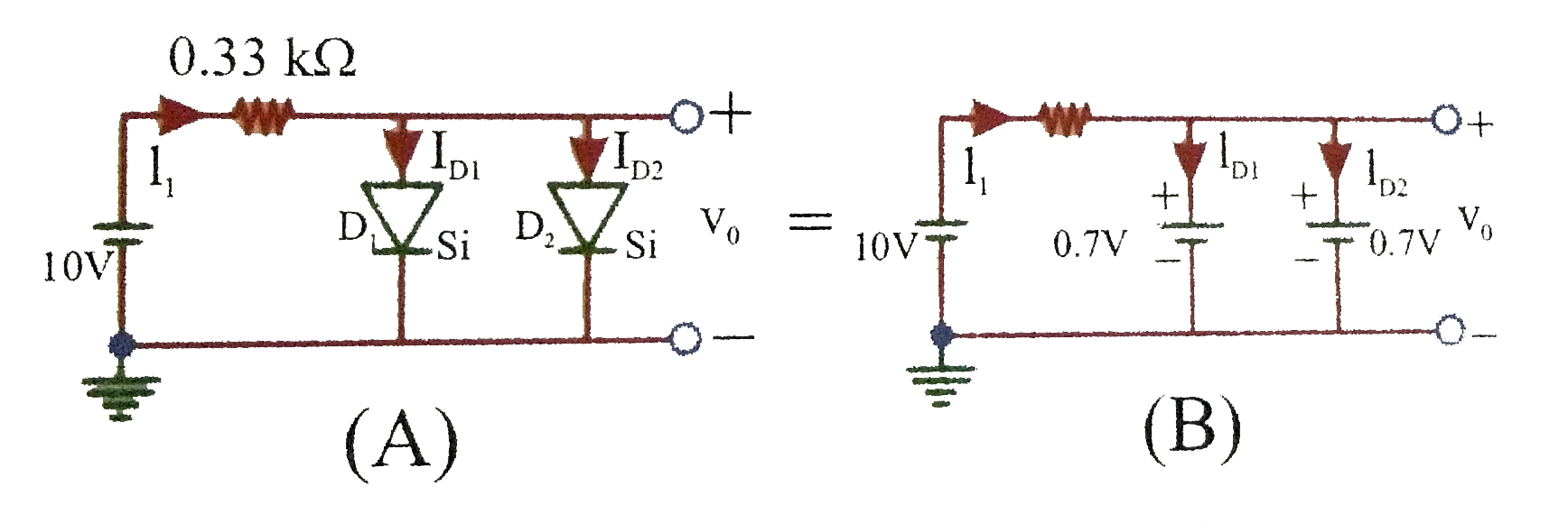
05:15View SolutionIn the circuit shown in figure (1), the `V_(0),I_(1),I_(D_(1))`, and `I_(D_(3))` are respectively.
(A) 03:45View Solution
For a junction diode, the ratio of forward current `(I_(f))` and reverse current is.
[`I_(e)` = electronic charge,
`V` = voltage applied across junction,
`k` = Boltzmann constant
`T` = temperature in kelvin].01:43View Solution
EXERCISE -2 (H.W) (JUNCTION DIODES) questions and complete solutions for chapter SEMICONDUCTOR ELECTRONICS of NARAYANA PHYSICS (HINGLISH) of Class 12
All Exercises from NARAYANA Class 12 PHYSICS SEMICONDUCTOR ELECTRONICS
- ADDITIONAL EXERCISE (ASSERTION AND REASON TYPE QUESTIONS :)
- C.U.Q (APPLICATION OF JUNCTION DIODE AS RECTIFIER)
- C.U.Q (INTRINSIC AND EXTRINSIC SEMICONDUCTORS)
- C.U.Q (LOGIC GATES)
- C.U.Q (SPECIAL PURPOSE P-N JUNCTION DIODES)
- EVALUATE YOURSELF-1
- EVALUATE YOURSELF-2
- EVALUATE YOURSELF-3
- EVALUATE YOURSELF-4
- EXERCISE -1 (C.W) (APPLICATION OF JUNCTION DIODE AS RECTIFIER)
- EXERCISE -1 (C.W) (INTRINSIC AND EXTRINSIC SEMICONDUCTORS)
- EXERCISE -1 (C.W) (JUNCTION DIODE)
- EXERCISE -1 (C.W) (LOGIC GATES)
- EXERCISE -1 (C.W) (TRANSISTORS)
- EXERCISE -1 (H.W) (APPLICATION OF JUNCTION DIODE AS RECTIFIER
- EXERCISE -1 (H.W) (INTRINSIC AND EXTRINSIC SEMICONDUCTORS)
- EXERCISE -1 (H.W) (JUNCTION DIODE)
- EXERCISE -1 (H.W) (LOGIC GATES)
- EXERCISE -1 (H.W) (TRANSISTORS)
- EXERCISE -2 (C.W) (APPLICATIONS OF JUNCTION DIODE AS RECTIFIER)
- EXERCISE -2 (C.W) (JUNCTION DIODES)
- EXERCISE -2 (C.W) (LOGIC GATES)
- EXERCISE -2 (C.W) (TRANSISTORS)
- EXERCISE -2 (C.W) INTRINSIC, EXTRINSIC SEMICONDUCTONS)
- EXERCISE -2 (H.W) (APPLICATIONS OF JUNCTION DIODE AS RECTIFIER)
- EXERCISE -2 (H.W) (INTRINSIC, EXTRINSIC SEMICONDUCTORS)
- EXERCISE -2 (H.W) (JUNCTION DIODES)
- EXERCISE -2 (H.W) (LOGIC GATE)
- EXERCISE -2 (H.W) (TRANSISTORS)
- EXERCISE -3
- EXERCISE-4
- ILLUSTRATION
