Complete Solutions to EXERCISE-4 of chapter SEMICONDUCTOR ELECTRONICS of Class 12 book with complete answers and questions
| Class 12 | PHYSICS |
| Chapter | SEMICONDUCTOR ELECTRONICS |
| NARAYANA | EXERCISE-4 |
| Number Of Questions | 35 |
| Academic Year | 2023-24 |
Which inpurity is doped in Si to form N-type semicondutor ?
View SolutionIn a semiconducto
View SolutionThe energy band gap is maximum in
01:58View SolutionThe part of a transistor which is most heavily doped to produce large number of majority carriers is
02:17View SolutionBy increasing the temperature the specific resistance of a conductor and a semiconductor
06:42View SolutionAt absolute zero , Si acts as
01:26View SolutionA strip of copper and another of germanium are cooled from room temperature to 80 K. The resistance of
01:34View SolutionIn the middle of the depletion layer of a reverse - biased `p - n ` junction , the
04:48View SolutionThe difference in the variation of resistance with temperature in a metal and a semiconductor arises essentially due to the difference in the
02:33View SolutionA piece of copper and another of germanium are cooled from room temperature to 77 K, the resistance of -
02:14View SolutionThe manifestation of band structure in solids is due to
05:41View SolutionEnergy band in solids are a consequence of
01:31View SolutionWhen forward bias is applied to a `P-N` junction, then what happence to the potential barrier `V_(B)`, and the width of charge depleted region `x`?
01:35View SolutionWhen NPN transistor is used as an amplifier
02:42View SolutionFor a transistor amplifier in common emitter configuration for load impedance of `1 k Omega. (h_(fe) = 50 and h_(oe) = 25 xx 10^(-6))` the current gain is
02:00View SolutionThe electrical conductivity of a semiconductor increases when electromagnatic radiation of wavelength shorter than 2480 nm is incident on it. The band gap (in eV) for the semiconductor is `[hc=1242 eV nm]`
01:34View SolutionIn a full wave rectifier circuit operating from `50 Hz` mains frequency , the fundamental frequency in the ripple would be
00:58View SolutionIn a common-base amplifier, the phase difference between the input signal voltage and output voltage is :
01:30View SolutionA solid which is not transperent to visible light and whose conductivily increase with temperature is formed by
01:35View SolutionIf the ratio of the concentration of electron to that of holes in a semiconductor is `(7)/(5)` and the ratio of current is `(7)/(4)` then what is the ratio of their drift velocities ?
01:57View SolutionIn a common base mode of transistor, collector current is `5.488 mA` for an emitter current of `5.60mA`. The value of the base current amplification factor `(beta)` will be :
01:48View SolutionIf the lattice constant of this semiconductor s decreases, then which of the following is correct ?
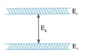 00:53View Solution
In the following, which one of the diodes is reverse biased ?
01:39View SolutionThe circuit has two oppositely connected ideal diodes in parallel. What is the current flowing in the circuit?
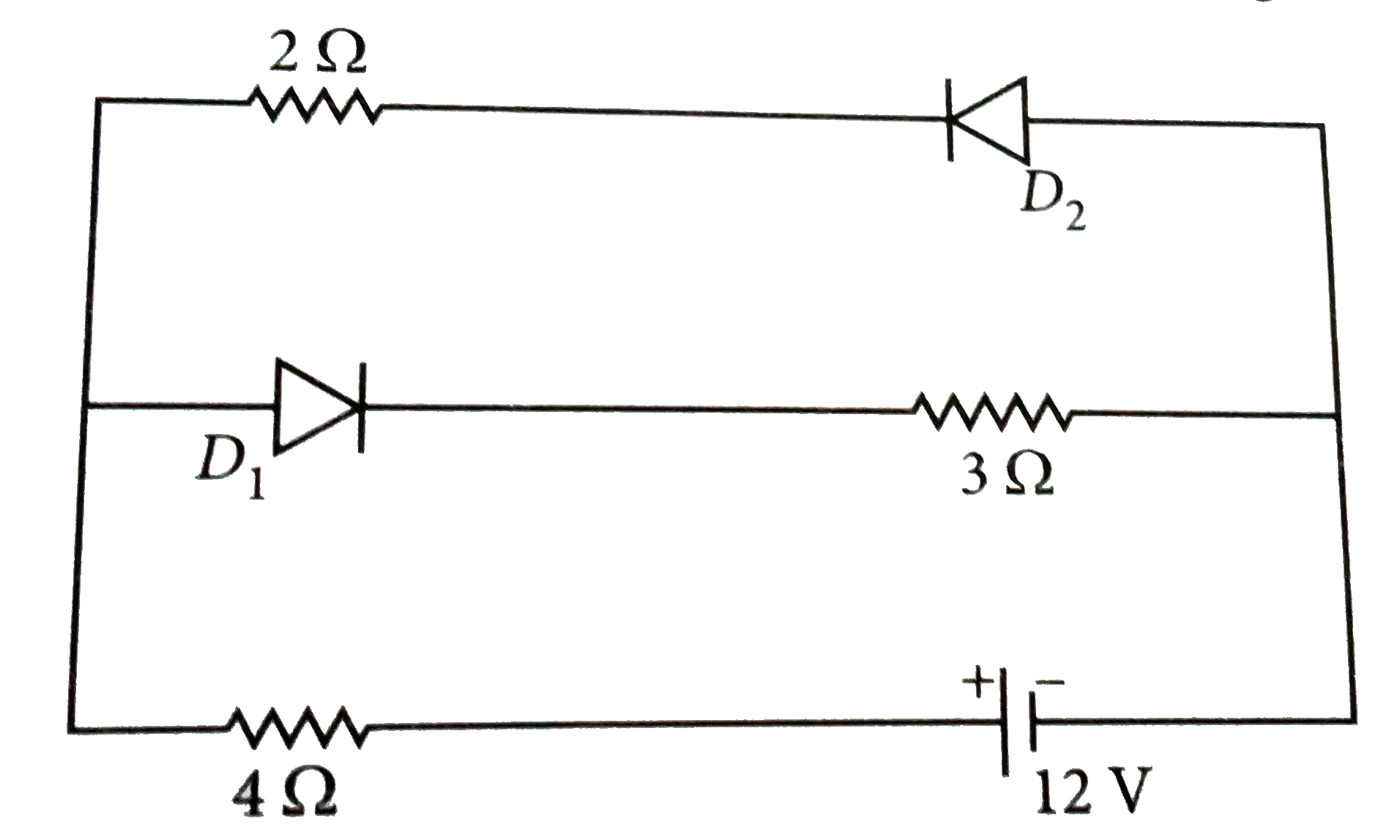 04:15View Solution
Carbon, silicon and germanium have four valence electrons each. The most appropriate statement for these elements (at room temperature) is
02:21View SolutionIf a pn junction dide, a square input signal of 10 V is applied as shown

then the outuput signal across `R_(1)` will be01:33View SolutionIn the circuit below, A and B represent two inputs and C represents the output.
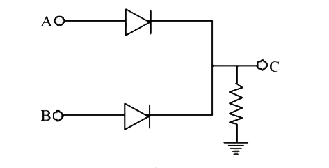
The circuit represents04:38View SolutionA `p-n` junction `(D)` shown in the figure can act as a rectifier. An alternating current source `(V)` is connected in the circuit.
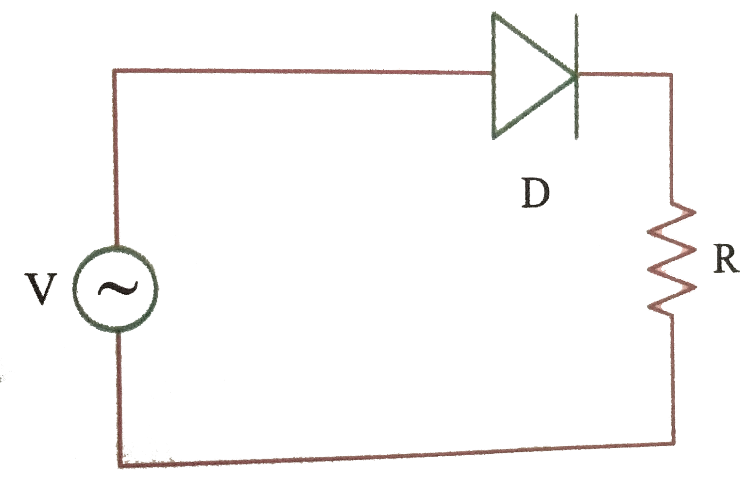 .01:55View Solution
The logic circuit shown has the input waveforms 'A' and 'B' as shown. Pick out the correct output waveform
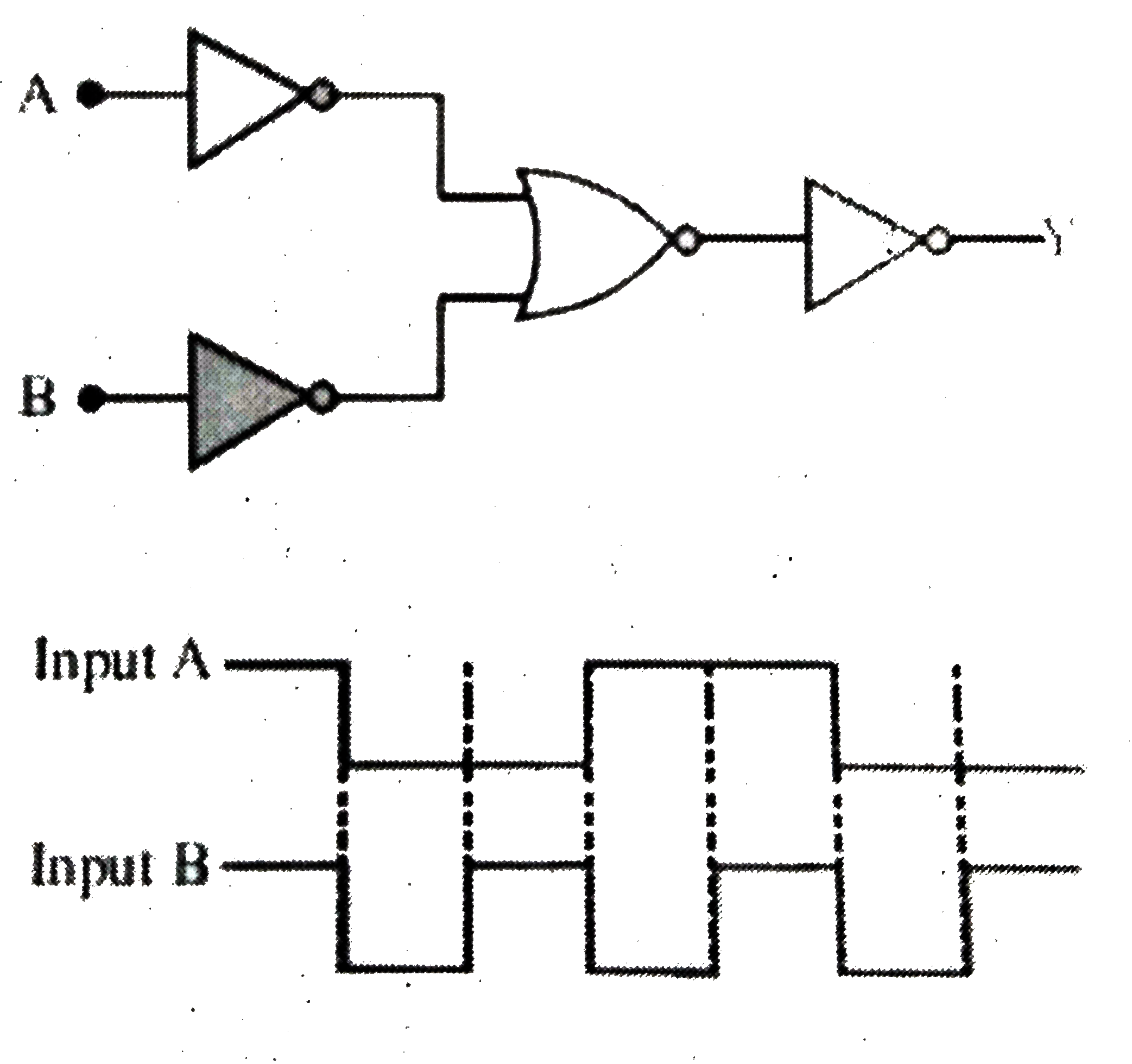 03:52View Solution
The combination of gates shown below yields
 02:21View Solution
Truth table for system of four NAND gates as shown in figure is
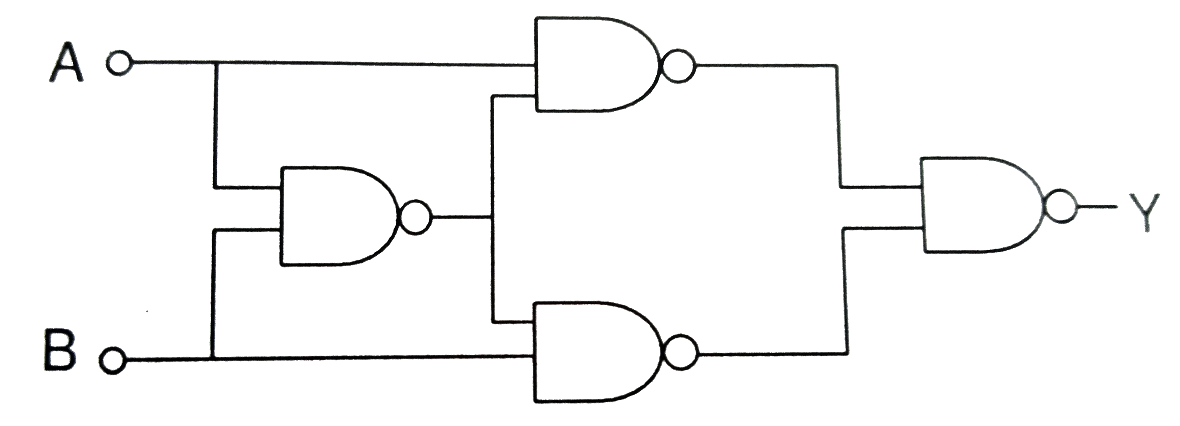 03:44View Solution
A diode detector is used to detect an amplitude modulated wave of `60%` modulation by using a condense of capacity `250` picofarad in parallel with a load resistance `100` kilo ohm find the maximum modulated which could be find the maximum modulated frequency which could be detected by it
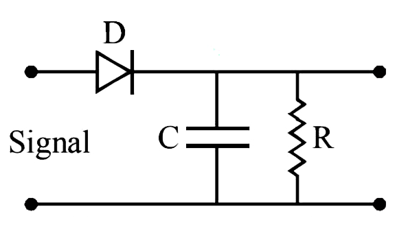 02:20View Solution
The `I-V` characteristic of an `LED` is.
01:30View SolutionThe currect voltage relation of diode is given by `1=(e^(1000 V//T)-1) mA`, where the applied voltage V is in volt and the temperature T is in degree Kelvin. If a student makes an error measuring `+-0.01 V` while measuring the current of `5 mA` at `300 K`, what will be error in the value of current in mA?
02:58View SolutionThe forward biased diode connection is
02:30View Solution
EXERCISE-4 questions and complete solutions for chapter SEMICONDUCTOR ELECTRONICS of NARAYANA PHYSICS (HINGLISH) of Class 12
All Exercises from NARAYANA Class 12 PHYSICS SEMICONDUCTOR ELECTRONICS
- ADDITIONAL EXERCISE (ASSERTION AND REASON TYPE QUESTIONS :)
- C.U.Q (APPLICATION OF JUNCTION DIODE AS RECTIFIER)
- C.U.Q (INTRINSIC AND EXTRINSIC SEMICONDUCTORS)
- C.U.Q (LOGIC GATES)
- C.U.Q (SPECIAL PURPOSE P-N JUNCTION DIODES)
- EVALUATE YOURSELF-1
- EVALUATE YOURSELF-2
- EVALUATE YOURSELF-3
- EVALUATE YOURSELF-4
- EXERCISE -1 (C.W) (APPLICATION OF JUNCTION DIODE AS RECTIFIER)
- EXERCISE -1 (C.W) (INTRINSIC AND EXTRINSIC SEMICONDUCTORS)
- EXERCISE -1 (C.W) (JUNCTION DIODE)
- EXERCISE -1 (C.W) (LOGIC GATES)
- EXERCISE -1 (C.W) (TRANSISTORS)
- EXERCISE -1 (H.W) (APPLICATION OF JUNCTION DIODE AS RECTIFIER
- EXERCISE -1 (H.W) (INTRINSIC AND EXTRINSIC SEMICONDUCTORS)
- EXERCISE -1 (H.W) (JUNCTION DIODE)
- EXERCISE -1 (H.W) (LOGIC GATES)
- EXERCISE -1 (H.W) (TRANSISTORS)
- EXERCISE -2 (C.W) (APPLICATIONS OF JUNCTION DIODE AS RECTIFIER)
- EXERCISE -2 (C.W) (JUNCTION DIODES)
- EXERCISE -2 (C.W) (LOGIC GATES)
- EXERCISE -2 (C.W) (TRANSISTORS)
- EXERCISE -2 (C.W) INTRINSIC, EXTRINSIC SEMICONDUCTONS)
- EXERCISE -2 (H.W) (APPLICATIONS OF JUNCTION DIODE AS RECTIFIER)
- EXERCISE -2 (H.W) (INTRINSIC, EXTRINSIC SEMICONDUCTORS)
- EXERCISE -2 (H.W) (JUNCTION DIODES)
- EXERCISE -2 (H.W) (LOGIC GATE)
- EXERCISE -2 (H.W) (TRANSISTORS)
- EXERCISE -3
- EXERCISE-4
- ILLUSTRATION
