Complete Solutions to Exercise of chapter SEMICONDUCTORS of Class 11 book with complete answers and questions
| Class 11 | PHYSICS |
| Chapter | SEMICONDUCTORS |
| RESONANCE | Exercise |
| Number Of Questions | 29 |
| Academic Year | 2023-24 |
p-n junction is
View SolutionThe depletion region of a P-N diode, under open circuit condition contains
View SolutionWhich is the wrong statement in following sentence? A device in which P and N type semiconductors are used is more useful then a vacuum tube because-
View SolutionThe contact potential at the junction site in a P-N junction is-
View SolutionA square wave (-1 to +1V) is applied to a P-N junction diode as shown. Draw the output wave form across the diode which is assumed to be ideal-

View Solution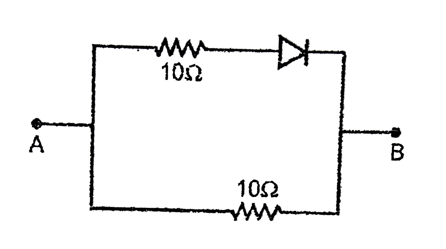
If `V_(A)` and `V_(B)` denote the potentials of A and B, then the equivalent resistance between A and B in the adjoint electric circuit is
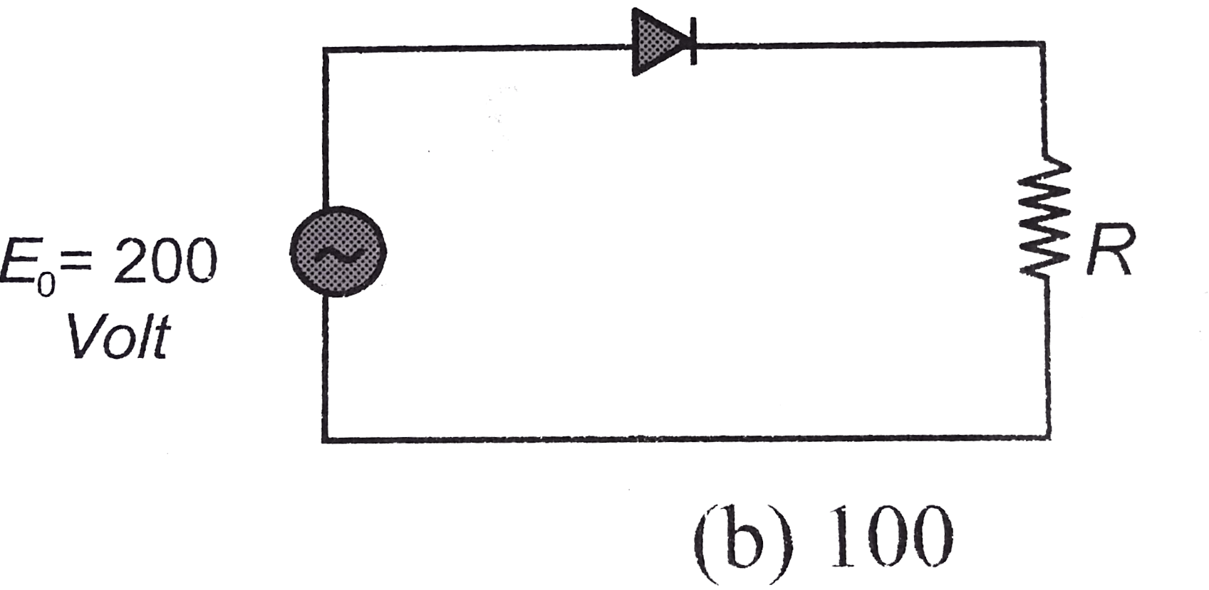
View SolutionA sinusoidal voltage of peak value `200` volts is connected to a diode and resistor `R` in the circuit shown so that half wave rectification occurs. If the forward resistance of the diode is negligible compared to `R` the `rms` voltage (in volt) across `R` is approximately
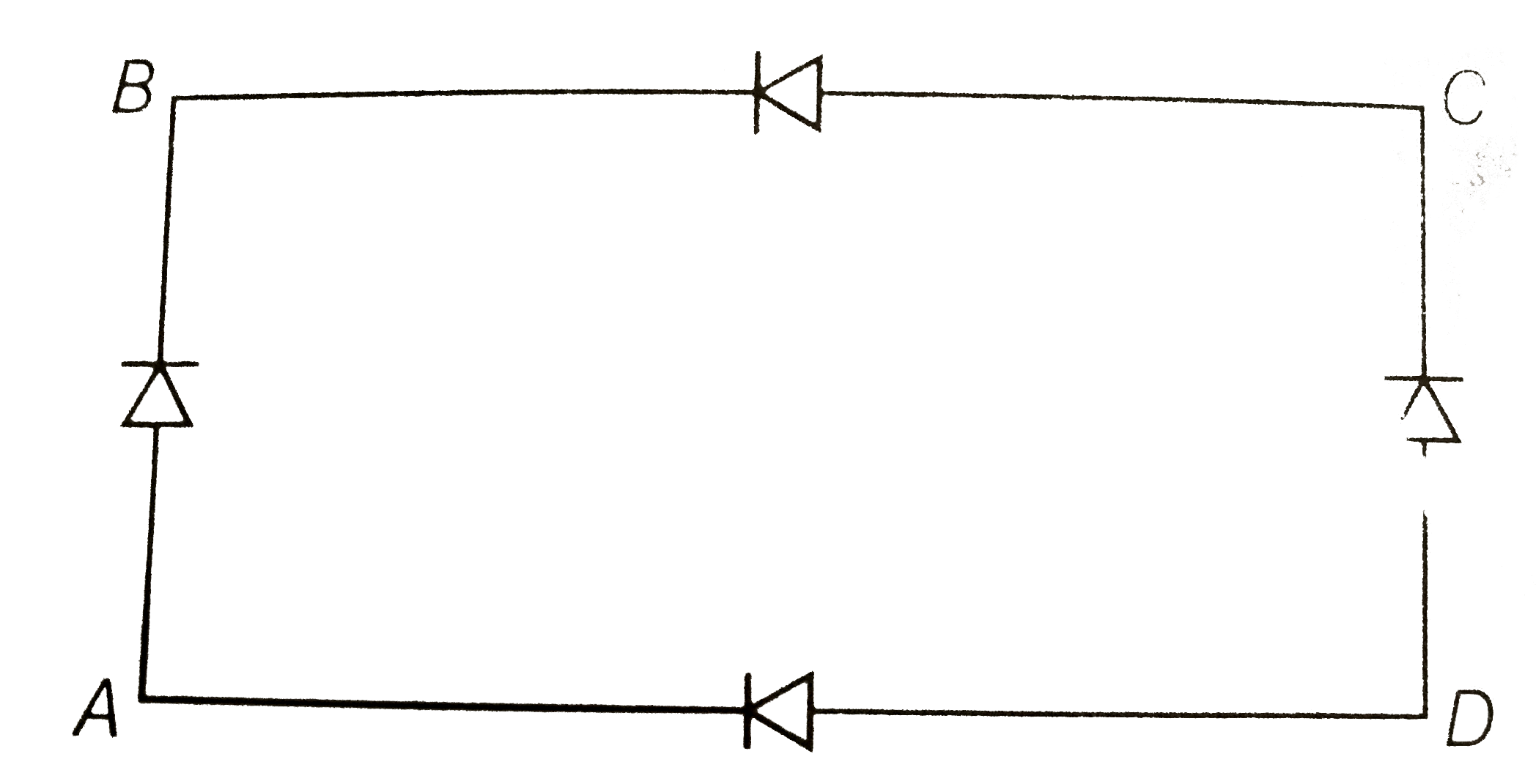
View SolutionIn figure the input is across the terminals A and C and the output is across B and D. Then the output is
View Solution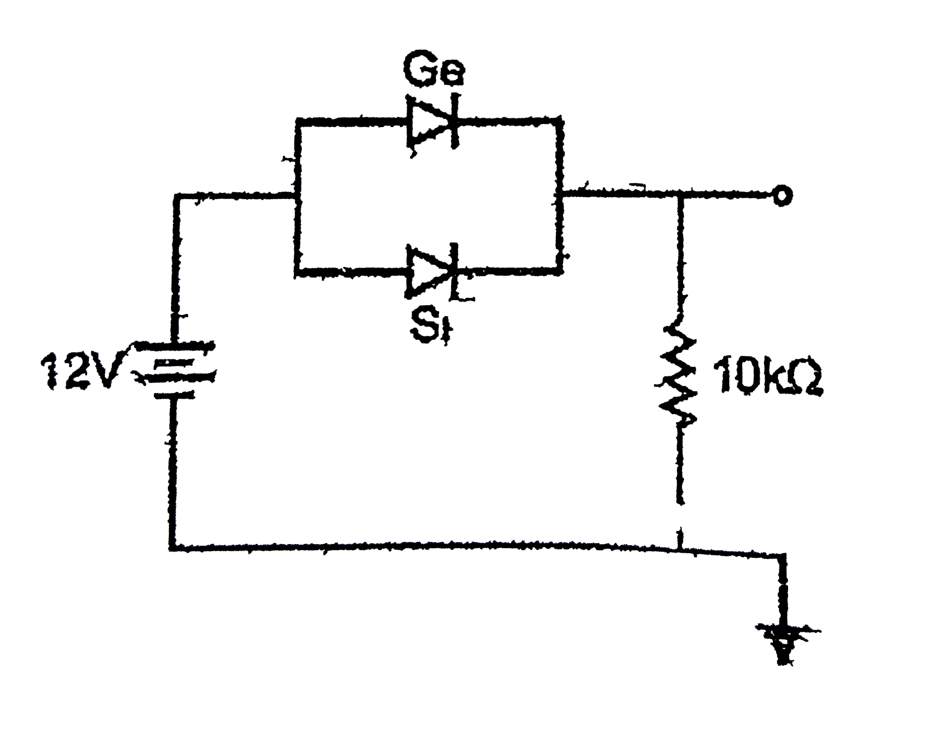
Two junction diodes one of germanium (Ge) and other of sillicon (Si) are connected as shown in figure to a battery of emf 12 V and a load resistance `10kOmega` the germanium diode conducts at 0.3 V and silicon diode at 0.7 V. When a current flows in the circuit, The potential of terminal Y will be
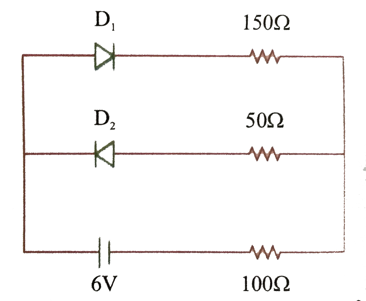
View SolutionThe circuit shown in figure (1) Contains two diodes each with a forward resistance of `50 ohm` and with infinite reverse resistance. If the battery voltage is `6 V`, the current through the `100 ohm` resistance is.
 .
.
View SolutionThe part of the transistor which is heavily doped to produced large number of majority carriers is
View SolutionThe difference in the variation of resistance with temperature in a metal and a semicondcutor arises essentially due to the difference in the
View SolutionWhen `p-n` junction diode is forward biased, then
View SolutionThe electrical conductivity of a semiconductor increases when electromagnetic radiation of wave length shorter than 2480 nm is incident on it. The band gap (in eV) for semiconductor is
View SolutionIn a common base amplifier the phase difference the input signal voltage and the output voltage is
View SolutionWith an ac input from 50 Hz power line, the ripple frequency is
View SolutionIf the ratio of the concentration of electrons and that of holes in a semiconductor is 7/5 and the ratio of their currents is 7/4, then the ratio of their drift velocities is
View SolutionIn a common-base of mode of transistor, the collector current is 5.488 mA for an emitter current of 5.60 mA. The value of the base current amplification factor (2) will be:
View SolutionA working transitor with its three legs marked `P, Q and R` is tested using a multimeter No conduction is found between `'P', Q `by connecting the common (negative) terminal of the multimeter to `R`and the other (positive) terminal to P or `Q` some resistance is seen on the multimeter . Which of the following is true for the transistor ?
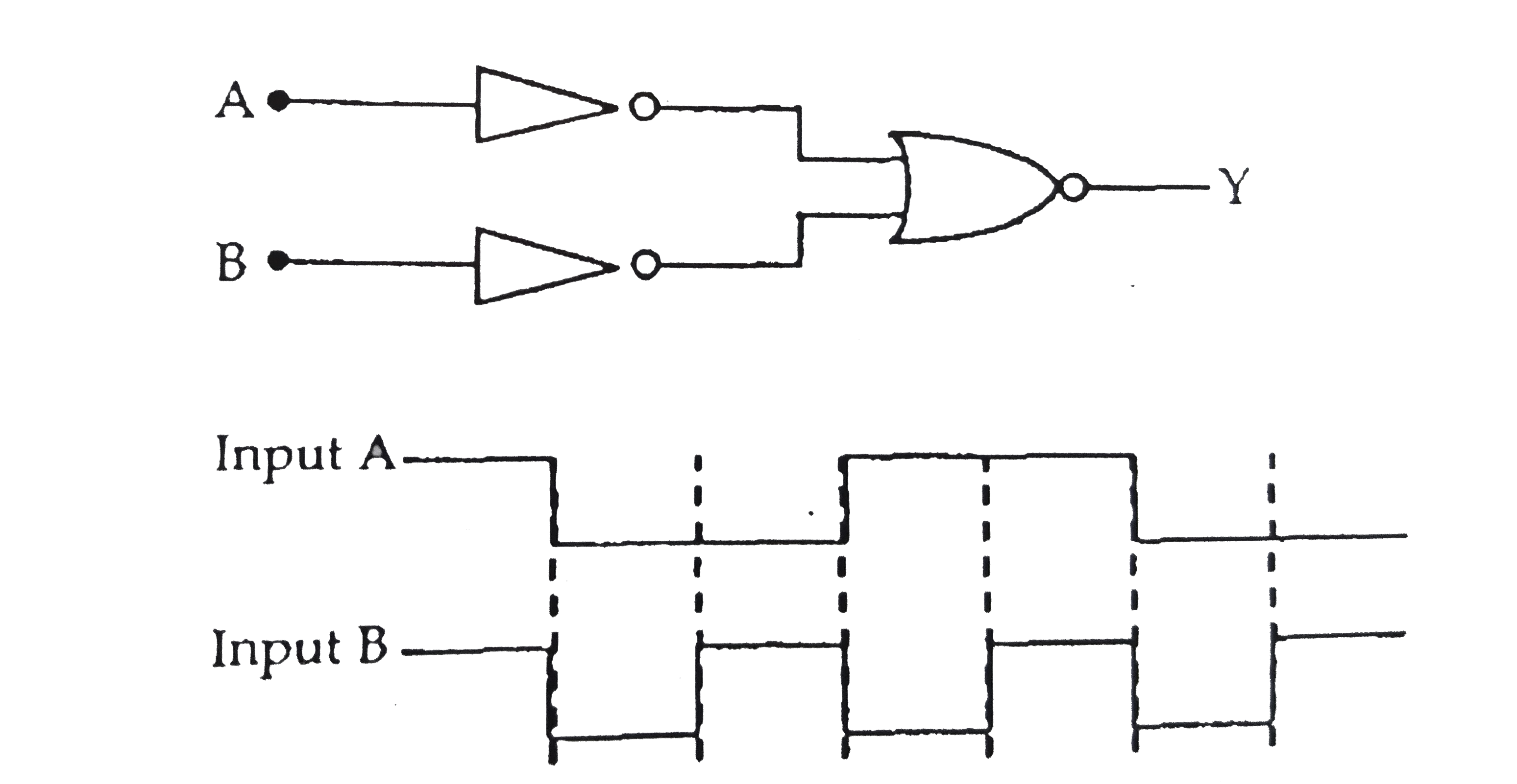
View SolutionThe logic circuit shown below has the input waveforems 'A' and 'B' as shown. Pick out the correct output waveform
View SolutionIn a …. Biased P-N junction the net flow holes is from N-region to the P-region?
View SolutionIn a p–n junction photo cell, the value of the photo electromotive force produced by monochromatic light is proportional to: -
View SolutionCarbon, silicon and germanium have four valence electrons each. These are characterised by valence and conduction bands separated by energy band gap respectively equal to `(E_g)_C, (E_g)_(Si), and (E_g)_(Ge)`. Which of the following statements is true?
View SolutionFor a transistor amplifier, the voltage gain
View SolutionIn a transistor connected in common emitter mode, `R_C=4 kOmega, R_1=1 kOmega, I_C=1 mA and I_B=20 muA`. The voltage gain is
View SolutionIn the figure shown `R_B = 500K Omega, R_C = 8K Omega, V_BB= 10.6 V` and `V_(C C) = 20V`. The current amplification factor of the transistor is 100 and `V_BE = 0.6` volt then which of the following is false?
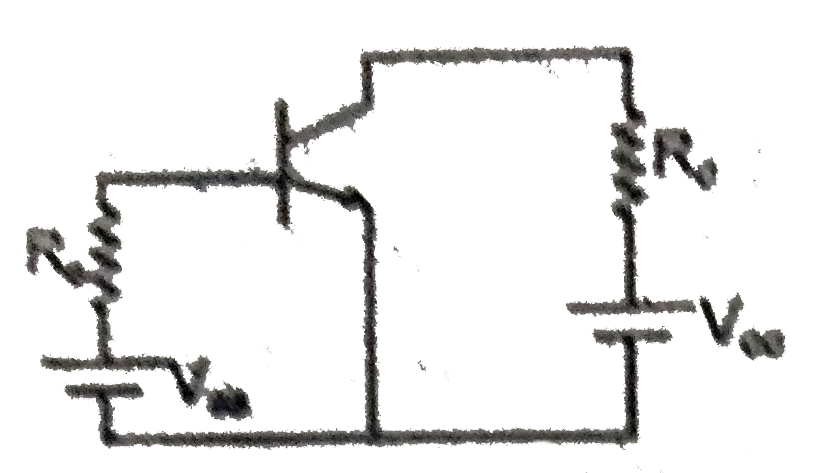
View SolutionWhich of the following statement is true for a p-n-p transistor when used in an amplifier circuit?
View SolutionA resistance R is connected at the n terminal of a p-n junction in series. An AC voltage is applied across this circuit. Which of the following are true for the circuit?
View SolutionFor a transistor,`alpha = 0.9`, the value of `beta` is
View Solution
Exercise questions and complete solutions for chapter SEMICONDUCTORS of RESONANCE ENGLISH of Class 11