Complete Solutions to EXERCISE of chapter SEMICONDUCTORS of Class 11 book with complete answers and questions
| Class 11 | PHYSICS |
| Chapter | SEMICONDUCTORS |
| TARGET PUBLICATION | EXERCISE |
| Number Of Questions | 100 |
| Academic Year | 2023-24 |
CONDUCTORS HAVE___electrical conductivity as conductivity as compared to insulators.
View SolutionOUT OF THE FOLL.semiconductors, which of them is an example of compound semiconductors?
View Solutionwhen the temperature of a semiconductor is increased , its electrical conductivity___.
View Solutionmetals are good conductors of heat as compared to the insulators because
View Solutionfor a given solid,closely spaced energy levels of all electros in a particular orbit is called
View Solutionin insulators,
View Solutionthe energy band gap is maximum in
View Solutionthe band gap in germanium and silicon in eV are
View Solutionthe main distinction between conductors,semiconduct ors and insulators is concerned with
View Solutionif the temperature of a semi condutror is incressed, then the forbidden gp will
View Solutionthe most commonly used semi caonductors are
View Solutiona pure semiconductor
View Solutionthr ratio of no.of holes and no. of conduction electrons in an intrinsic semiconductor is
View Solutionat absolute zero temerature , a crystal of pure germanium
View Solutionwhich of the foll. Is NOT a 'donor' impurity?
View SolutionPure silicon should be doped with which of the foll. Impurity atoms to make a p-type semiconductor?
View Solutiona n-type semiconductor is formed
View SolutionRegarding p-type and n-type semiconductors,which of the foll..statements is true?
View Solutiona semiconductor is damaged by a strong current ,because of
View Solutionbond in n and p type semiconductor is
View Solutionin germanium crystal.a hole is provided by a___impurity.
View Solutionon doping germanium metal with a little amount of indium, one gets
View Solutiondoping materials are caled impurities because
View Solutiona hole in a semiconductcorr is rather diff. from an electron because it has
View Solutionsuitable impurities are added to a semiconductor depending on its use. This is done to
View SolutionThe donor atoms have energy level
View SolutionThe diode is called an electronic valve since
View Solutionin a semiconductor diode, the abrrier potential offers opposition to only
View Solutionin a p -n junction , there is no appreciable current if
View SolutionThe potential barrier developed in a junction diode opposes
View Solutionwhen a p junction dioode is forward biased, the flow of cufrent across the junction is mainly
View Solutionin p-n junction diode, holesdiffuse from p-region to n-region because
View SolutionDepletion layer in the P-N junction is caused by
View SolutionThe potential difference developed across the junction due to migration of majority carriers is called___
View Solutionin asemiconductor diode, reverse bia current is due to drift of ffree electons and holes caused by
View Solutiona p-n junction diode is sai to be forwarded biased whwn a potential diff. applied across p and n region makes
View Solutionan ideal diode
View Solutiona p-n junction diode cannot be used
View Solutionleakage current in ajunction diode
View SolutionAssertion : Semiconductor devices are thermally stable. Reason: No heating effects occur in semiconductor
View SolutionElectron Holes pairs are generated in photodiode
View SolutionPhotocurrent in a photodiode depends upon
View SolutionUsually Si is used in the designing of photodiodes because
View SolutionA Solar Cell
View SolutionCombination of solar cells designed to increase the electric power output is called
View Solutionsolar cell producs photo voltage whwn incident light has eenrgy
View SolutionThe color of light emitted by LED depends on
View SolutionThe barrier potential in LED depends on type of
View Solutionthe brightness of LED can be controlled by
View Solutionchoose the INCORRECTT statement
View Solutionthermistor is a temperature sensitive___device
View Solutionin case of a semiconductor, which of the foll. Statements is wrong?
View Solutionelectrical conductivity of a silicon is ___
View Solutionthe conductivity `(sigma)`of a solid is given by [n=no. of carriers per unit volume, q= charge on th carrirs, `mu`=mobility of carriers]
View Solutionelectrical conductivity of a semiconductor
View Solutionat room temperature,electrical conductivity of semiconductor is
View SolutionAssertion:the resistivity of a semiconductor increases with temperature. Reason: in a conducting solid,the rate of collisions between free electrons and ions increases with increase of temperature
View Solutionin a good conductor the energy gap between the conduction band and the valence band is
View Solutionenergy band in solids are a consequence of
View Solutionthree semiconductors are arranged in the incresing order of their gap as follows. The correct arrangement is
View SolutionAssertion: the energy gap between the valence band and conduction band is greater in silicon than in germanium. Reason: thermal energy produces fever minority carriers in silicon than in ghermanium
View Solutionwhich one of the energy band diagrams shown in the figure coresponds to that of semiconductor?
View Solutionelectronic configuration of silicon is___.
View Solutionin a semiconductor,
View SolutionIn an intrinsic semiconductor
View Solutionlet `n_p` and `n_e` be the no. oh holes and conduction electrons in a semicondutcor . Then,
View Solutionresistivity of pure geramanium crystal at room temperature in order of
View Solutionin a pure silicon (`n_i = (10^16)/m^3) crystal at 300 k ,`10^21` atoms of phosphorous are added percubic meter. The new hole concetaration wil be.
View Solutionto a germanium sample , trace sof gallium are added as an imourity. The resuyltant sample would behave like
View Solutionwhen phosphorous and antimony are mixed in germanium , then
View SolutionIntrinsic semiconductor is electrically neutral. Extrinsic semiconductor having large no. of current carriers would be
View SolutionGermanium and Silicon belong to the 14th group of periodic table. Hence each atom of Ge or Si will have
View SolutionAfter Doping , resistivity of a semiconductor
View Solutionthe electrical conductivity of a p-type semiconductor is determined by the no. of
View SolutionIn Extrinsic Semiconductors
View SolutionThe majority charge carriers in P-type semiconductors are
View Solutiona p-type semiconductor can be obtained by adding
View Solutionif `n_e` aand `n_h` are the no. of electrrons and holes in a semiconductor heavily doped with phosphorous , then
View Solutionwhen n-type of semiconductor is heated
View SolutionA diode converts A.C. voltage into a /an
View Solutionthe order of thickness of delpting region in p-n junction is
View Solutionp-n junction diode works as an insulator , if connected
View Solutionin a semiconductor diode, a p-side is earthed and n-side is applied a potential of -2V , the diode will
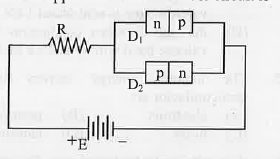
View Solutionfigure shows ttwo p-n junction diodes alond with aresistance R and a dc battery E. the path of flow of appreciable current in the circuit is,

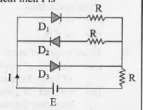
View Solutionin the foll. Circuit of PN junction , diodes `D_1, D_2 and D_3` are ideal then I is

View SolutionOF THE DIODES SHOWN IN the foll. Diagrams, which one is reverse biased?
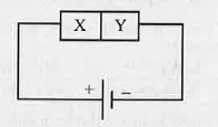
View Solutiona semiconductorX is made by doping a germanium crytsal with arsenic (z=33). A second semiconductor Y is made by doping germanium with indium (z=49) . The two are joined end to end and connected to a battery as shown in fiure. Which of the foll. statement is correct?

View Solutionthe dominant mecahnisms for motion of chargecarriers in forward and reverse biased silicon p-n junctions are
View Solutionserious draback of the semiconductors devices is __
View Solutionin LED, to avoid damage to the diode ___is used
View Solutionin LED, intensity of emitted light
View Solutionwhich of the foll. Is NOT an appliction of photodiode?
View Solutionin a p-n junction photo cell, the value of photo-electromotive force produced by monochromatic light is proportional to
View SolutionAssertion :light emitting diode (LED) emits spontaneous radiation reason: LED are forward biased p-n junction
View Solutionthermistors may have
View Solutionwhich of the foll. Graphs represents NTC thermistors
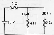
View Solutionthe circuit has two oppositely connected ideal diodes in parallel. What is the curenet ideal dioddes in parallel. What is the current foll. In the circuit?

View Solutiona p-n junction diode when forward biased has a drop of 0.4 V which is assumed to be independent of currebnt A. a current excess of 10mA through the diode damages (burns) the diode .if we want to use a 2 V battrey to forwqard bias the diode, what should be the avlue of resistor used in series with the diode so thatthe maximum current does NOT exced 5mA?
View Solutionfor a photodiode , the forbidden energy gap` (E_8)`of the material used is 2.8eV and wavelength of radiations (`lambda`) incident on it is 5780 A. then the emission of electrons is possible when incident radiation have
View Solutionif the band gap between valence band and conduction band in a matereial is 5.0 eV , then the material is
View Solution
EXERCISE questions and complete solutions for chapter SEMICONDUCTORS of TARGET PHYSICS (MARATHI ENGLISH) of Class 11