Complete Solutions to NUMERICALS of chapter ELECTRONIC DEVICES of Class 12 book with complete answers and questions
| Class 12 | PHYSICS |
| Chapter | ELECTRONIC DEVICES |
| SUPPORT MATERIAL | NUMERICALS |
| Number Of Questions | 7 |
| Academic Year | 2023-24 |
In a p-n junction, width of depletion region is 300 nm and electric field of `7 xx 10^(5) V//m` exists in it.
(i) Find the height of potential barrier.
(ii) What should be the minimum kinetic energy of a conduction electron which can diffuse from the n-side to the p-side?View SolutionAn LED is constructed from a p-n junction based on a certain semi-conducting material whose energy gap is 1.9 eV. Then, the wavelength of the emitted light is
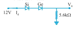
02:42View SolutionDetermine `V_(0)` and `I_(d)` for the network.
 View Solution
A p-n junction is fabricated from a semiconductor with band gap of `2.8eV`. Can it detect a wavelength of `6000nm`?
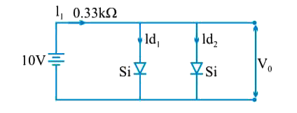
03:02View SolutionDetermine `V_(0), I_(d1)` and `I_(d2)` for the given network. Where `D_(1)` and `D_(2)` are made of silicon.
 03:06View Solution
Pure Si at 300 K has equal electron `(n_(e))` and hole `(n_(h))` concentrations of `1.5xx10^(16)m^(-3)` doping by indium increases `n_(h)` to `4.5xx10^(22)m^(-3)`. Caculate `n_(e)` in the doped Si-
01:20View SolutionThe solar radiation spectrum shows that maximum solar intensity is near to energy hv = 1.5 eV. Answer the following:
(i) Why are SI and GaAs are preferred materials for solar cells.
(ii) Why CdS or CdSe are preferred materials for solar cells.
(iii) Why we do not use materials like PbS (Eg ~ 0.4 eV).View Solution
NUMERICALS questions and complete solutions for chapter ELECTRONIC DEVICES of CBSE COMPLEMENTARY MATERIAL PHYSICS (HINGLISH) of Class 12
