Complete Solutions to MCQs of chapter SEMICONDUCTORS of Class 12 book with complete answers and questions
| Class 12 | PHYSICS |
| Chapter | SEMICONDUCTORS |
| MARVEL | MCQs |
| Number Of Questions | 100 |
| Academic Year | 2023-24 |
What is the forbidden energy gap (in joule) for a Germanium crystal ?
View SolutionThere is a small energy gap between the conduction and valence bands of
View SolutionCopper and silicon is cooled from 300 K to 60 K, the specific resistance
View SolutionCarbon , silicon and germanium have four valence elcectrons each . These are characterised by valence and conduction bands separated by energy band - gap respectively equal to ` (E_g)_(c) (E_g)_(si) ` and ` (E_g)_(Ge) `. Which of the following statements ture ?
View SolutionThe highest energy level which can be occupied by an electron in valence band at OK is known as
View SolutionAt absolute zero , Si acts as
View SolutionThe difference in the variation of resistance with temperature in a metal and a semiconductor arises essentially due to the difference in the
View SolutionChoose only the wrong statement from the following :
View SolutionIn a good conductor the energy gap between the conduction band and the valence band is
View SolutionIn an insulator
View SolutionA strip of copper and another of germanium are cooled from room temperature to 80 K. The resistance of
View SolutionCarbon , silicon and germanium have four valence electrons each . At room temperature which one of the following statements is most appropriate ?
View SolutionThe probability of electrons to be found in the conduction band of an intrinsic semiconductor at a finite temperature
View SolutionThe level formed due to impurity atom, in the for hidden energy gap, very near to the valence band in a p-type semiconductor is called
View SolutionThe impurity atoms with which pure silicon should be doped to make a p - type semiconductor are those of
View SolutionWhat is the change in resistance and electrical coductivity of a semiconductor, when its temperature is increased ?
View SolutionThe forbidden energy band gap in conductors, semiconductors and insulators are `EG_(1), EG_(2)` and `EG_(3)` respectively. The relation among them is
View SolutionHow does potential barrier of a semiconductor vary with temperature?
View SolutionIn a semiconductor, the energy gap between the valence and conduction bands is 1. 1 eV. It is expressed in joules as
View SolutionThe mobility of mobile holes is less than that of mobile electrons because
View SolutionThe electrical conductivity of pure silicon can be increased by
View SolutionFind the 'wrong' statement from the following : In a semiconductor
View SolutionThe specimen of an intrinsic semiconductor contains `1.2xx10^15` holes/`m^3`. If it is doped by phosphorous atoms in a small proportion, then the number of holes/`m^3` in the doped semiconductor will
View SolutionA conductor, an insulator, a semiconductor and an alloy are heated by `20^@C` above the room temperature. Then there is an increase in the conductivity of the
View SolutionWhich is the wrong statement from the following?
View SolutionIn pure semiconductor, the number of conduction electrons is `6 xx 10^18` per cubic metre. How many holes are there in a sample of size 1 cm x 1 cm x 1 mm?
View SolutionA semiconductor is known to have an electron concentration of `6xx10^(12)` per cubic centimeter and a hole concentration of `8xx10^(13)` per cubic centimeter. Is this semiconductor N-type or P-type ?
View SolutionChoose the false statement from the following
View SolutionWhen the conductivity of a semiconductor is only due to breaking of covalent bonds, the semi conductor is called.
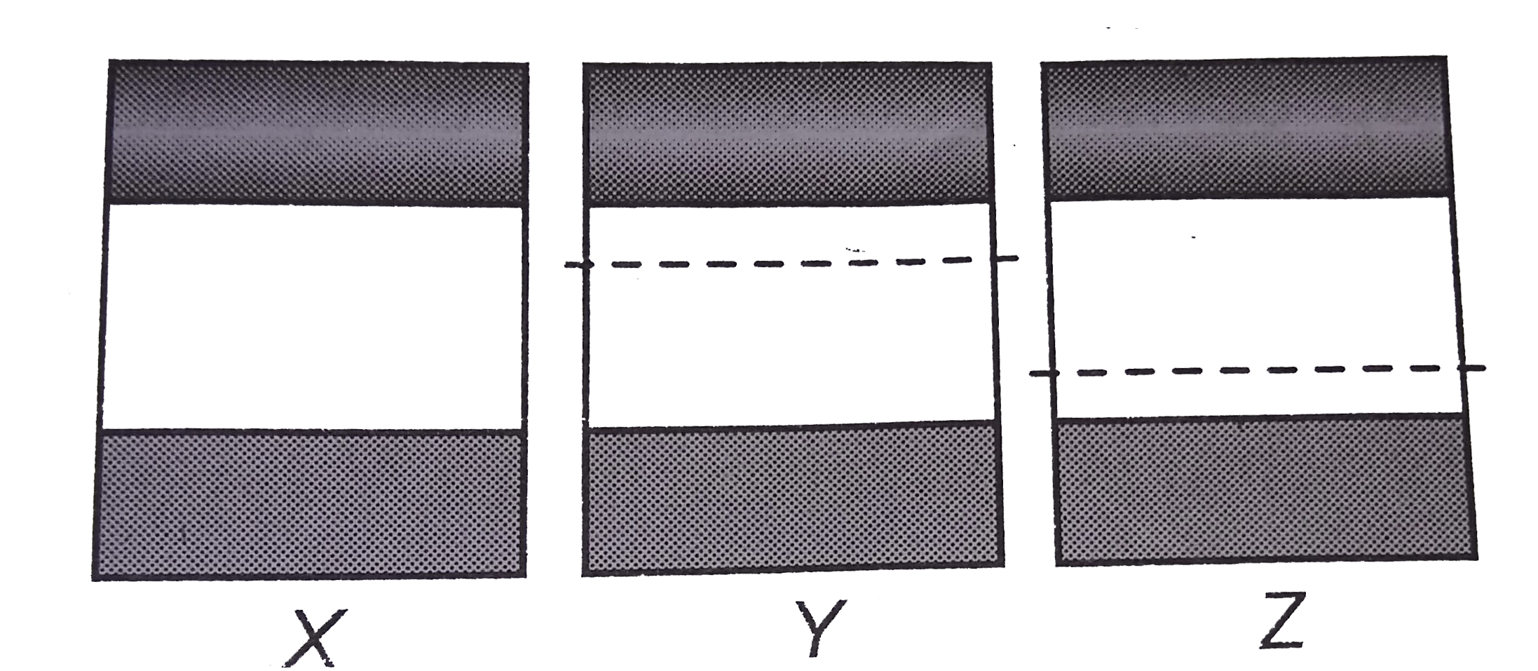
View SolutionThe energy band diagrams for three semiconductor samples of silicon are as shown. We can then assert that
View SolutionIn case of a semiconductor, which of the following statement is wrong?
View SolutionIntrinsic semiconductor is electrically neutral. Extrinsic semiconductor having large number of current carriers would be
View SolutionThe maximum wavelength of electromagnetic radiation, which can create a hole-electron pair in germanium. (Given that forbidden energy gap in germanium is 0.72 eV)
View SolutionIn a pure silicon `(n_(i)=10^(16)//m^(3))` crystal at `300K, 10^(21)` atoms of phosphorus are added per cubic meter. The new hole concentration will be
View SolutionThere are two Ge crystals A and B. Few aluminium atoms are added to A while few lndium atoms are added to B. Then
View SolutionBy increasing the temperature , the specific resistance of a conductor and a semiconductor
View SolutionIn semiconductors at a room temperature
View SolutionWhich of the following , when added as an impurity, into the silicon, produces n-type semiconductor ?
View SolutionA semiconductor has phosphorus as impurity, then it will have
View SolutionThe conductivity of a semiconductor increases with increase in temperature because
View SolutionIn a P -type semi-conductor, germanium is dopped with
View SolutionCarbon , silicon and germanium have four valence elcectrons each . These are characterised by valence and conduction bands separated by energy band - gap respectively equal to ` (E_g)_(c) (E_g)_(si) ` and ` (E_g)_(Ge) `. Which of the following statements ture ?
View SolutionThe electrical conductivity of a semiconductor increases when electromagnatic radiation of wavelength shorter than 2480 nm is incident on it. Find the band gap of the semiconductor. Given `h=6.63xx10^(-34)Js, and 1eV=1.6xx10^(-19)J`.
View SolutionIn the energy band diagram of a material shown below, the open circles and filled circles denote holes and electrons respectively. The material is

View SolutionA silicon specimen is made into a `P`-type semiconductor by dopping, on an average, one helium atoms per `5xx10^(7)` silicon atoms. If the number density of atoms in the silicon specimen is `5xx10^(28) at om//m^(3)` then the number of acceptor atoms in silicon per cubic centimeter will be
View SolutionThe energy gap of silicon is `1.14 eV`. The maximum wavelength at which silicon will begin absorbing energy is
View SolutionA `Ge` specimen is dopped with `Al`. The concentration of acceptor atoms is `~10^(21) at oms//m^(3)`. Given that the intrinsic concentration of electron hole pairs is `~10^(19)//m^(3)`, the concentration of electron in the speciman is
View Solutionif `n_(e)` and `v_(d)` be the number of electrons and drift velocity in a semiconductor. When the temperature is increased.
View SolutionWhen a potential difference is applied across, the current passing through
View SolutionA P-type sillicon semiconductor is made by adding one atom of indium per `5xx10^(7)` atoms of sillicon. If the number density of silicon is `25xx10^(28) "atom"//m^(3)`. Point the number of acceptor atoms in per cubic cm. of sillicon
View SolutionPure `Si` at `500K` has equal number of electron `(n_(e))` and hole `(n_(h))` concentration of `1.5xx10^(16)m^(-3)`. Dopping by indium. Increases `n_(h)` to `4.5xx10^(22) m^(-3)`. The doped semiconductor is of
View SolutionWhen a battery is connected to a `P`-type semiconductor with a metallic wire, the current in the semiconductor (predominantly), inside the metallic wire and that inside the bettery respectively due to
View SolutionIf the ratio of the concentration of electron to that of holes in a semiconductor is `(7)/(5)` and the ratio of current is `(7)/(4)` then what is the ratio of their drift velocities ?
View SolutionA semiconducting device is connected in a series circuit with a battery and a resistance.A current is found to pass through the circuit .If the polarity of the battery is reversed, the current drops to almost zero.The device may be
View Solution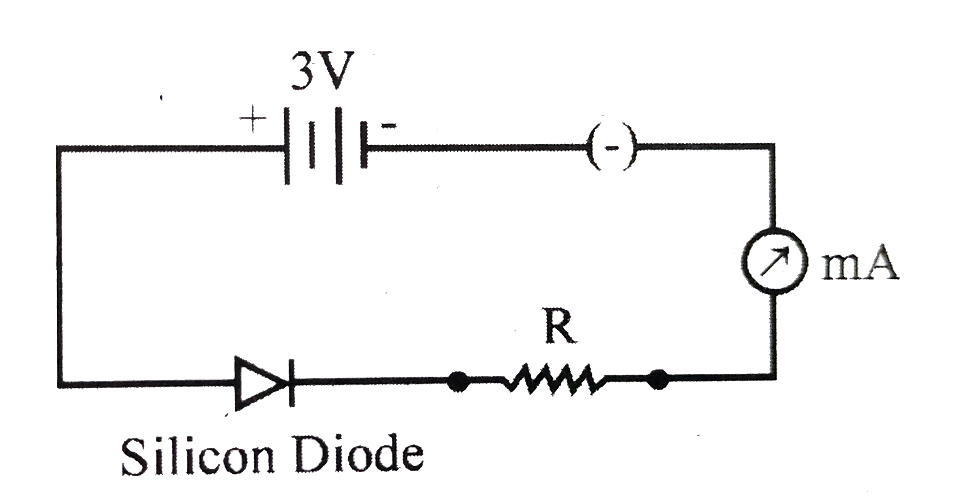
In the above circuit, the voltage drop across the resistance (R) is
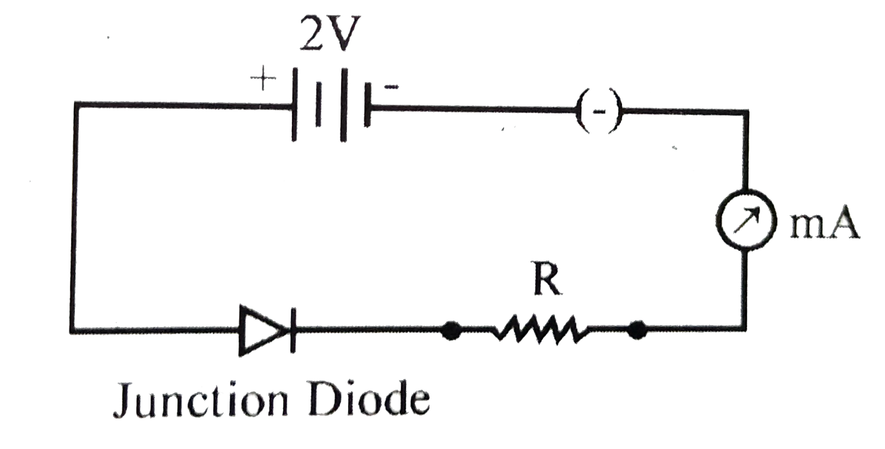
View SolutionSome current is flowing in the milli ammeter in the following circuit. If the applied voltage is increased from 2 V to 4 V, then
View SolutionWhen the forwward bias voltage of a diode is changed from `0.6` V to `0.7` V the current changes from 5 mA to 15 mA. Then its forward bias resistance is
View SolutionA half-wave rectifier is being used to rectify an alternating voltage of frequency 50 Hz. The number of pulses of rectified current obtained in one second is
View SolutionWhich of the following diodes is forward-biased ?
View SolutionIn which one of the following devices the reverse biased characteristics of a p-n junction diode are used?
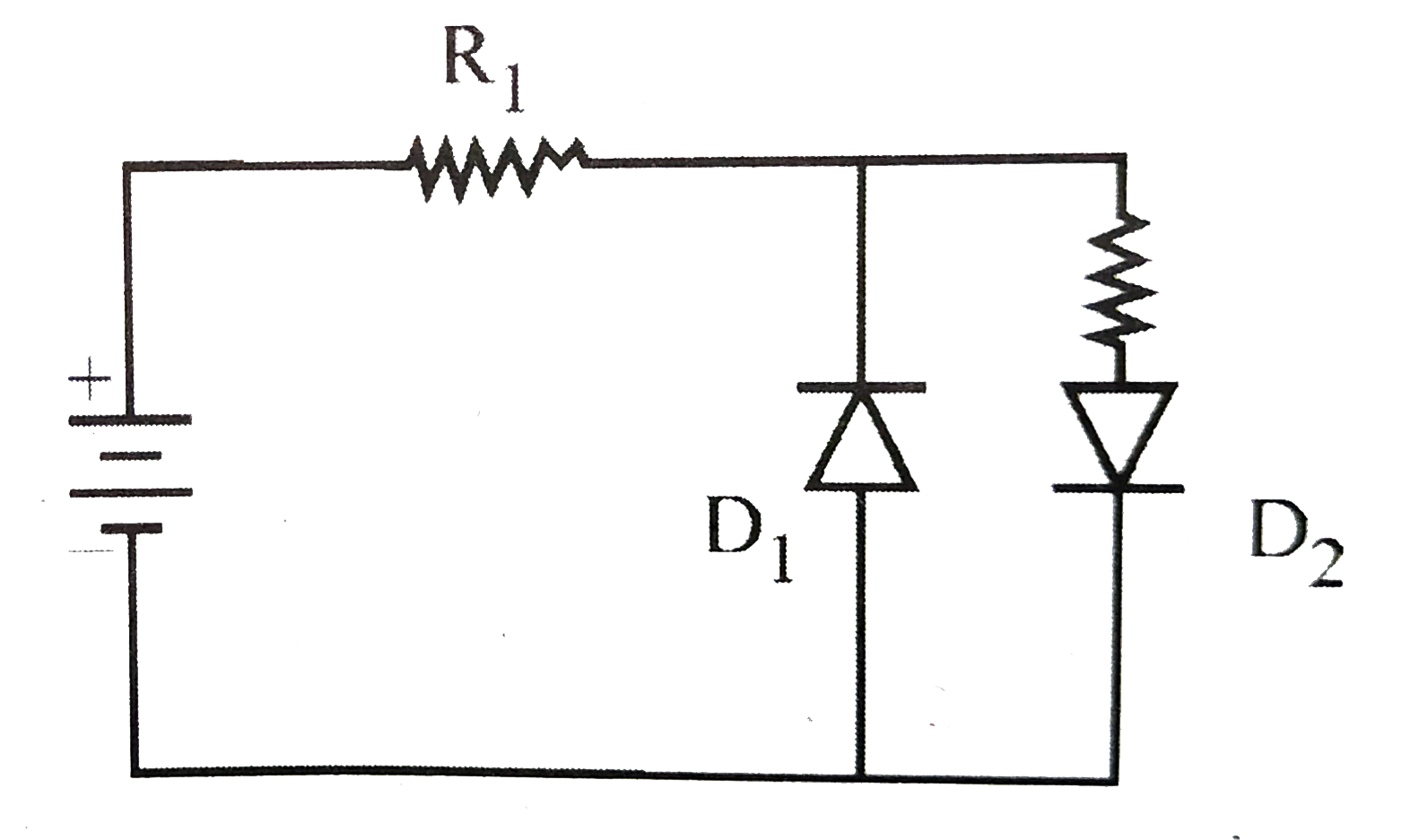
View SolutionIn the following circuit
View SolutionIf the forward voltage in a semiconductor diode is chaged form 0.5 V to 2 V, then the forward current changed by 1.5 mA. The forward resistance of diode will be-
View SolutionThe depletion region of a p - n junction is formed
View SolutionIn half - wave rectification, what is the output frequency, if the
input frequency is 50 Hz ? What is the output frequency of a full - wave rectifier
for the same input frequency ?
View SolutionWhen the resistance between p and n regions is very high then the p-n junction diode acts as
View SolutionIn a p - n junction, electric conduction takes place due to
View SolutionThe current obtained from a simple filterless reactifier is
View SolutionIn the case of a p-n junction diode, if the reverse bias is very high, there is a sudden large increase in current. In this case the value of reverse bias voltage is known as
View SolutionWhat happens to the depletion region of a p-n junction ?
View SolutionWhat is the resistance of the diode circuit between A and B. (`D_1` and `D_2` are ideal diodes)
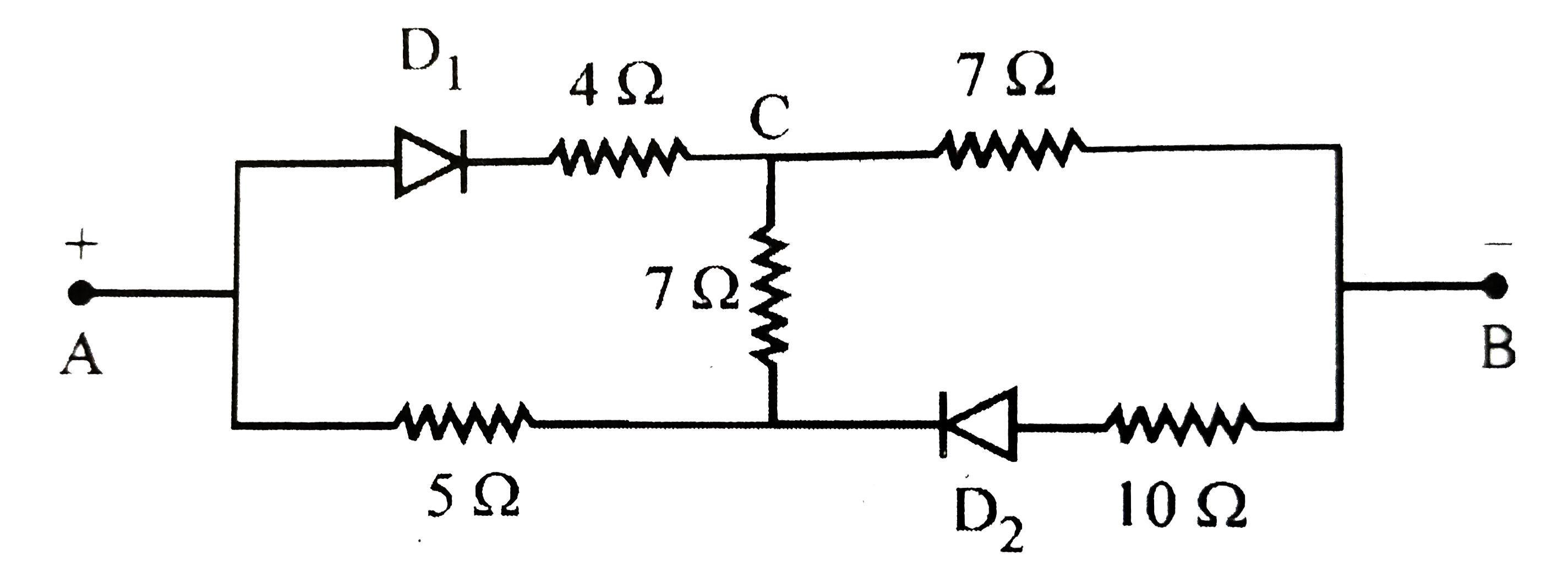
View SolutionIn a p-n junction, the thickness of the depletion region is `10^(-5)` m. What is the P.D. that should be applied across it, to produce an electric field of intensity `10^5` V /m ?
View SolutionA potential barrier of 0.3 V exists across a p-n junction. If the depletion region is 1 `mu`m wide, what is the intensity of electric field in this region?
View SolutionThe potential barrier of a semiconductor is 0.6 Vat room temperature. What is the approximate value of its potential barrier, if the temperature is increased by `20^@C`?
View SolutionThe current through the diode in the given circuit is
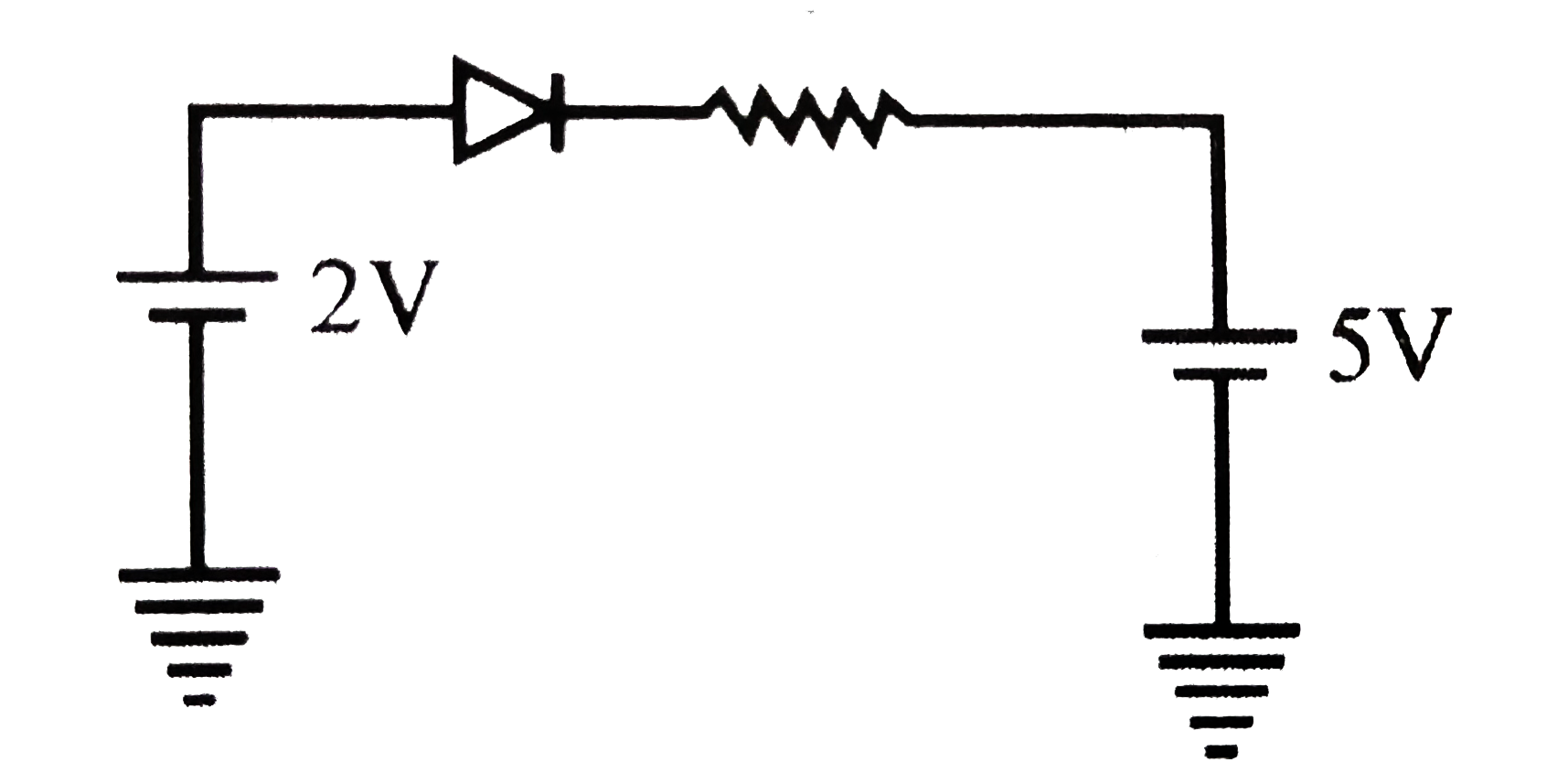
View SolutionWhen the `P` end of `P-N` junction is connected to the negative terminal of the battery and the `N` end to the positive terminal then diode behaves as
View SolutionThe electrical circuit used to get smooth `dc` output from a rectifier circuit is called
View SolutionWhat is the current through an ideal p-n junction diode shown in figure below ?
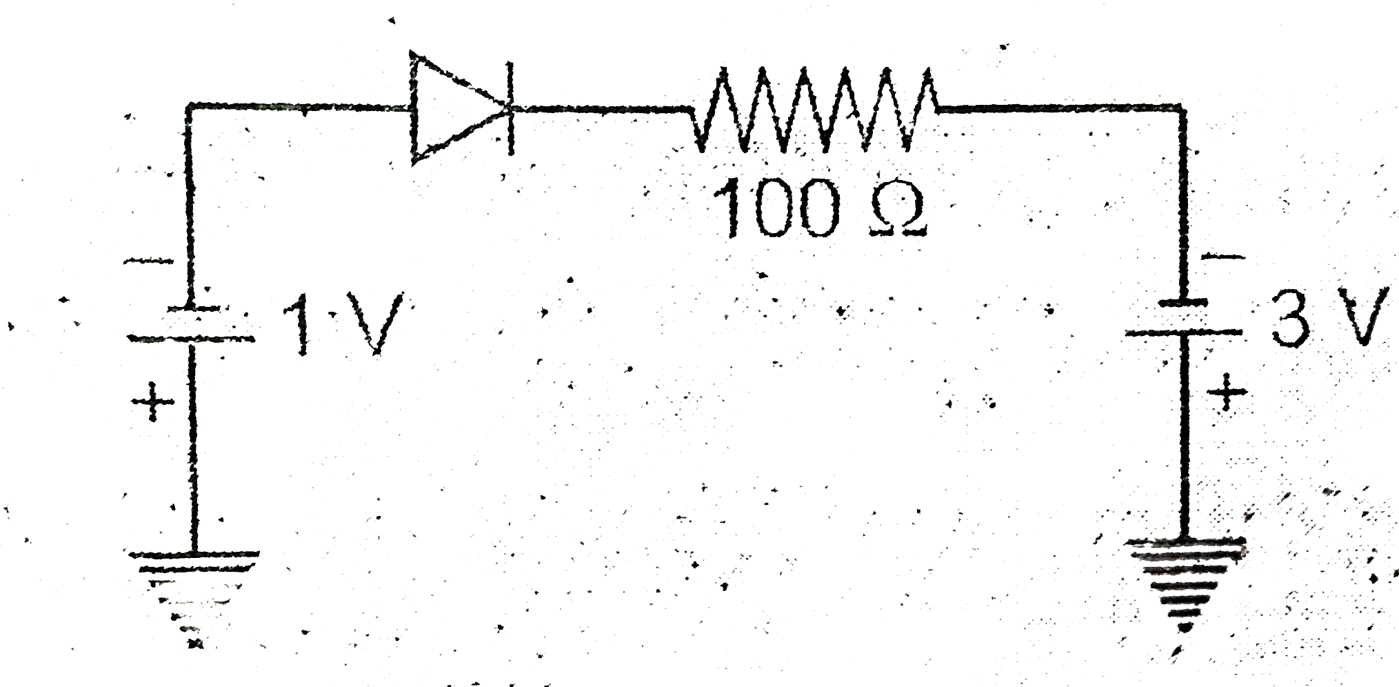
View SolutionWhat is the current in the following diode circuit?

View SolutionThe depletion layer in `P-N` junction region is caused by
View SolutionA junction diode has a resistance of 25 `Omega` when forward biased and 2500 `Omega` when reverse biased. What is the current in the diode, for the arrangement shown ?

View SolutionWhen forward bias is applied to a `P-N` junction, then what happence to the potential barrier `V_(B)`, and the width of charge depleted region `x`?
View SolutionIn an unbiased p-n junction,
View SolutionThe diode shown in the circuit is a silicon diode. The potential difference between the points `A` and `B` will be
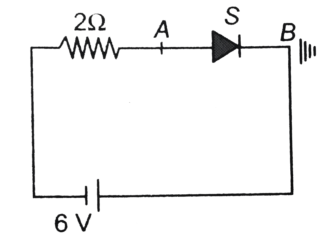
View SolutionA diode having potential difference `0.5 V` across its junction which does not depend on current, is connected in series with resistance of `20 Omega` across source. If `0.1A` passes through resistance then what is the voltage of the source?
View SolutionIn a reverse biased diode, when the applied voltage changes by `1V`, the current is found to change by `0.5muA`. The reversebiase resistance of the diode is
View SolutionBarrier potential of a `p-n` junction diode does not depend on
View SolutionWhen `p-n` junction diode is forward biased then
View SolutionIf a full wave rectifier circuit is operating from `50 Hz` mains, the fundamental frequency in the ripple will be
View SolutionApplication of a forward biase to a `p-n` junction:
View SolutionThe barrier potential of a `p-n`-junction depends on
(i) Type of semiconductor material
(ii) Amount of doping
(iii) Temperature
which of the following is correct?
View SolutionA recutifier is used to
View SolutionFreuency of given AC signal is 50 Hz. When it connected to a half - wave rectifier, then what is the number of output pulses given by rectifier within one second ?
View SolutionThe depletion layer in a p-n junction diode is `10^(-6)` m wide and its knee potential is 0.5 V, then the inner electric field in the depletion region is
View SolutionA semiconducting device is connected is series with a battery, a resistance and a microammeter. It is found that there is practically no current in the circuit. But if the polarity of the battery is reversed, there is a sudden increase in the current. The device may be
View SolutionThe dominant mechanisms for motion of charge carriers in forward and reverse biased silicon `P-N` junction are
View SolutionFor the diode D, the forward resistance is zero and the backward resistance is infinite. It is connected in a D.C. circuit as shown in the figure. The potential difference between X and Y is

View SolutionIn the middle of the depletion layer of a reverse - biased `p - n ` junction , the
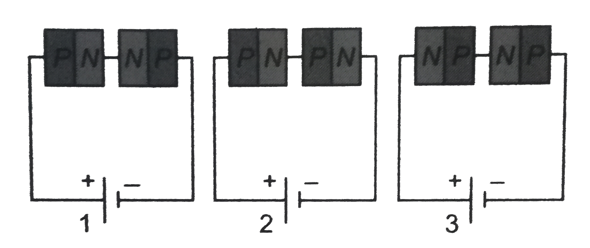
View SolutionTwo `PN`-junction can be connected in series by three different methods as shown in the figure. If the potential difference in the junction is the same, then the correct connection will be
View SolutionIn a p- n junction diode not connected to any circuit,
View SolutionThe peak voltage in the output of a half-wave diode rectifier fed with a sinusiodal signal without filter is `10 V`. The `dc` component of the output voltage is
View Solution
MCQs questions and complete solutions for chapter SEMICONDUCTORS of MARVEL PHYSICS (HINGLISH) of Class 12