Complete Solutions to ILLUSTRATION_TYPE of chapter SOLIDS AND SEMICONDUCTOR DEVICES of Class 12 book with complete answers and questions
| Class 12 | PHYSICS |
| Chapter | SOLIDS AND SEMICONDUCTOR DEVICES |
| SL ARORA | ILLUSTRATION_TYPE |
| Number Of Questions | 56 |
| Academic Year | 2023-24 |
In a pure semiconductor the number of conduction electrons is `6xx10^(19)`per cubic metre.How many holes are there in a sample of size `1cmxx1cmxx1mm?`
View SolutionFind the maximum wavelength of electromagnetic radiation which can create a hole-electron pair in germanium.The band gad in germanium os 0.65eV.
View SolutionA p-type semoconductor has acceptor levels `57meV `above the valence band. Find the maximum wavelength of light which can create a hole.
View SolutionA semiconductor has equal electron and hole concentration of `2 xx 10^(8)m^(-3)`. On doping with a certain impurity, the hole concertraction increases to `4 xx 10^(10)m^(-3)`. (i) What type of semiconductor is obtained on doping? (ii) Calculate the new electron hole concentration of the semiconductor. (iii) How does the energy gap vary with doping?
View SolutionA semiconductor has an electron concentration of `0.45 xx 10^(12) m^(-3)` and a hole concentration of `5.0 xx 10^(20) m^(-3)`. Calculate its conductivity. Given electron mobility `= 0.135 m^(2) V^(-1) s^(-1)`, hole mobility `= 0.048 m^(2) V^(-1) s^(-1)`,
View SolutionA semiconductor is known to have an electron concentration of `5xx10^(12) cm^(-3)` and a hole concentration `8xx10^(13)cm^(-3) ` Is the semi-conductor n-type or p-type? What is the resistivity of the sample, if the electron mobility is `23,000 cm^(2) V^(-1)s^(-1)`? Take charge on electron, `e=1.6xx10^(-19) C`.
View SolutionDetermine the number density of donor atoms which have to be added to an intrinsic germanium semiconductor to produce an n-type semiconductor of conductivity `5Omega^(-1)cm^(-1)`, given that the mobility of electron in n-type germanium is `3900 cm^(2)V^(-1)s^(-1)`. Neglect the contribution of holes to conductivity.
View SolutionA battery of emf `2V` is connected across a block of length `0.1m` and area of cros-section `1xx10^(-4)m^(2)`. If the block is of intrinsic silocon at `300K`, find the electron and hole currents. What will be the magnitude of the total current? What will be the magnitude of the total current if germanium is used instead of silicon?
Given that for `Si` at `300K`: `mu_(e)=0.135m^(2)V^(-1)s^(-1),mu_(h)=0.048m^(2)V^(-1)s^(-1)` and intristic carrier concentration `n_(i)=1.5xx10^(16)m^(-3)`. For `Ge` at `300K: mu_(e)=0.39m^(2)V^(-1)s^(-1),mu_(h)=0.19m^(2)V^(-1)s^(-1)` and `n_(i)=2.4xx10^(19)m^(-3)`
View SolutionIf resistivity of pure silicon is `3000 Omega meter`, and the electron and hole mobilities are `0.12 m^(2)V^(-1)s^(-1)` and `0.045m^(2)V^(-1)s^(-1)` respectively, determine the resistivity of a specimen of the material when `10^(19)` atoms of phosphorous are added per `m^(3)` are also added. Given charge on electron `=1.6x10^(-19)C`.
View SolutionIn an intrinsic semiconductor the energy gap `E_(g) is 1.2 eV`. Its hole mobility is much smaller than electron mobility and independent of temperature. What is the ratio between conductivity at `600K` and `300K`? Assume that temperature dependence intrinstic concentration `n_(i)` is given by
`n_(i)=n_(0) exp ((-E_(g))/(2k_T))`, where `n_(0)` is a constant and `k_=8.62xx10^(-5)eV//K`.
View SolutionWhen the voltage drop across a `p.n` junction diode is increased from `0.65V` to `0.70V`, the change in the diode current is `5mA`. What is the dynamic resistance of the diode?
View SolutionFigure shos the characteristic curve of a junction diode. Determie the d.c. and a.c. resistance of the diode, when it operates at `0.3V`.
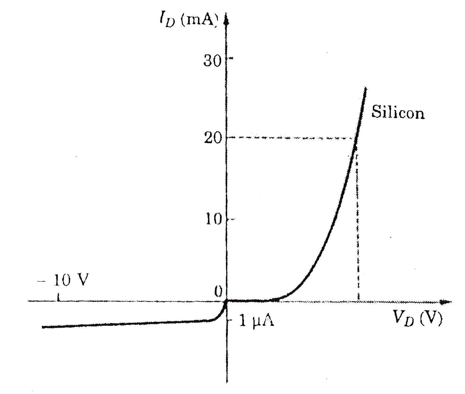
View SolutionThe volt-ampere characteristic of a silicon diode is shown in fig. Determine the resistance of the diode at (i) `I_(D)=20mA` and (ii) `V_(D)=-10V`.
View SolutionA `p-n` junction diode when forward biased has a drop of `0.5V` which is assumed to be independent of current. The current in excess of `10mA` through the diode produces a large Joule heating which damages (burns) the diode. If we want to use a `1.5V` battery to forward bias the diode, what should be the vlaue of resistor used in series with the diode so that the maximum current does not exceed `5mA`?
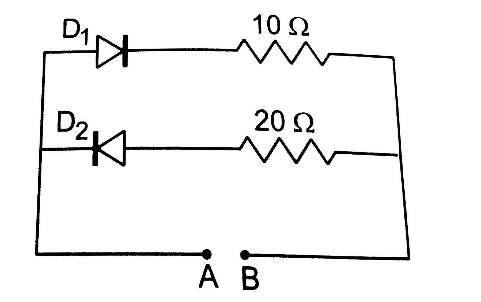
View SolutionA 2V battery may be connected across the points A and B as shown in figure. Assume that the resistance of each diode is zero in forward bias and infinity in reverse bias.Find the current supplied by the battery if the positive terminal of the battery is connected to (a) the point A (b)the point B.
View SolutionDraw the circuit to forward bias a diode. (The supply is `3V` and `100mA` battery). If the diode is made of silicon and knee voltage is `0.7V`, and a current of `20mA` passes through the diode, find the wattge of the resistor and the diode.
View SolutionIn figure what is the voltage needed to maintain `15V` across the load resistance `R_(L)` of `2K`, assuming that the series resistance `R` is `200Omega` and the zener requires a minimum current of `10mA` to work satisfactorily? What is the zener rating required?
View SolutionA potential barrier of 0.50V exists across a p-n junction.(a) If the depletion region is `5.0xx10^(-7)`m wide,what is the intensity of the electric field in this region?(b) An electron with speed`5.0xx10^(5)m s^(-1)`approaches the p-n junction form the n-side.With what speed will it enter the p-side?
View SolutionIn half - wave rectification, what is the output frequency, if the
input frequency is 50 Hz ? What is the output frequency of a full - wave rectifier
for the same input frequency ?
View SolutionThe turns ratio of a transformer used in a half wave rectifier ils `12:1`. The primary is connected to the power mains `220V, 50Hz`. Assuming the diode resistance in forward bias to be zero, calculate the d.c. voltage across the load.
View SolutionIn a centre trap full wave rectifier, the load resistance `R_(L)=1kOmega`. Each diode has a forward bias dynamic resistance of `10Omega`. The voltage across half the secondary winding is `220sin 314t`. Find (i) the peak value of current (ii) the dc value of current and (iii) the rms value of current.
View SolutionAssume that the silicon diode in the circui shown in fig. requires a minimum current of `1mA` to be above the knee point `(0.7V)` of its `I-V` characteristics. Aslo assume that the voltage across the diode is independent of current above the knee point.
(a) If `V_(B)=5V`, what should be the maximum value of `R` so that the voltage is above the knee point?
(b) If `V_(B)=5V`, what should be the value of `R` to estabilish the current of `5mA` in the circuit?
(c) What is the power dissipated in the resistance `R` and in the diode, when a current of `5mA` flows in the circuit at `V_(B)=6V`?
(d) If `R=1kOmega`, what is the minimum voltage `V_(B)` required to keep the diode above the knee point?
View SolutionIn a `p-n` junction diode, the currect `I` can expressed as `I=I_(0) exp((eV)/(2k_(B)T)-1)` where `I_(0)` is called the reverse saturation current, `V` is the voltage across the diode and is positive for forward bias and negative for reverse bias, and `I` is the current through the diode, `K_(B)` is the Boltzmann constant `(8.6 xx 10^(-5) eV//K)` and `T` is the absolute temperature. If for a given diode `I_(o) = 5 xx 10^(-12) A` and `T = 300 K`, then
(a) What will be the forward current at a formward voltage of `0.6V` ?
(b) What will be the increase in the current if the voltage across the diode is increased to `0.7 V` ?
( c) What is the dynamic resistance ?
(d) What will be current if reverse bias voltage changes from `1 V` to `2 V` ?
View SolutionIn a common emiter transistor circuit, if the collector-emitter voltages changes by `0.2V`, the collector current changes by `0.004mA`. What is the output resistance of the circuit,
View SolutionIf a change of `100 mu A` in the base current of an `n-p-n` transistor in `CE` causes a change of `10 mA` in the collector current, the `ac` current gain of the transistor is
View SolutionWhat is the change in the collector current, in a transistor of a.c. current gain 150 for a `100muA` change in its base current?
View SolutionA transistor has a current gasin of 30. If the collector resistance is `6kOmega`, input resistance is `1kOmega`, calculate its voltge gain?
View SolutionFor a transistor connected in common emitter mode, the voltage drop across the collector is `2V` and `beta` is 50. Find the base current is `R_(C)` is `2K`
View SolutionIn a transistor connected in a common emitter mode it has, `R_(c)=4kOmega, R_(i)=1kOmega, I_(c)=1mA and I_(b)= 20 muA.` Find the voltage gain.
View SolutionIn a silicon transistor, a change of `80mA` emitter current produces a change of `7.9mA` in the collector current. What change in the base current is necessary to produce an equivalent change in the collector current? Find the values of `alpha` and `beta`.
View SolutionTwo amplifiers are connected as shown in fig. Find `V_(0)` if `G_(1)=20, G_(2)=10` and `V_("in")=50,V. V_(Z)=10V` for each diode.

View SolutionA transistor has `alpha=0.95`. If the emitter current is `10mA`, what is (a) the collector current, (b) the base current and (iii) gain `beta`?
View SolutionThe input resistance of a silicon transistor is `665Omega`. Its base current is changed by `15muA` which results in the change in collector current by `2mA`. This transistor is used as a common emitter amplifier with a load resistance of `5kOmega`. What is the voltage gain of the amplifier.
View SolutionIn a silicon transistor, base current is changed by `20muA`. This result in a change of `0.02V` in base-emitter voltage and a change of `2 mA` in the collector current.
Find the input resistance, `beta_(a.c.)` and transconductance of the transistor.
The transistor is used as an amplifier with the load resistance `5k Omega`. What is the voltage gain of the amplifier?
View SolutionIn a transistor amplifier `beta=62, R_(L)=5000Omega` and internal resistance of the transistor `=500Omega`. Calculate the voltage amplification and power amplification.
View SolutionOutput characteristics of an n-p-n transistor in CE configuration is shown in the Fig. Determine
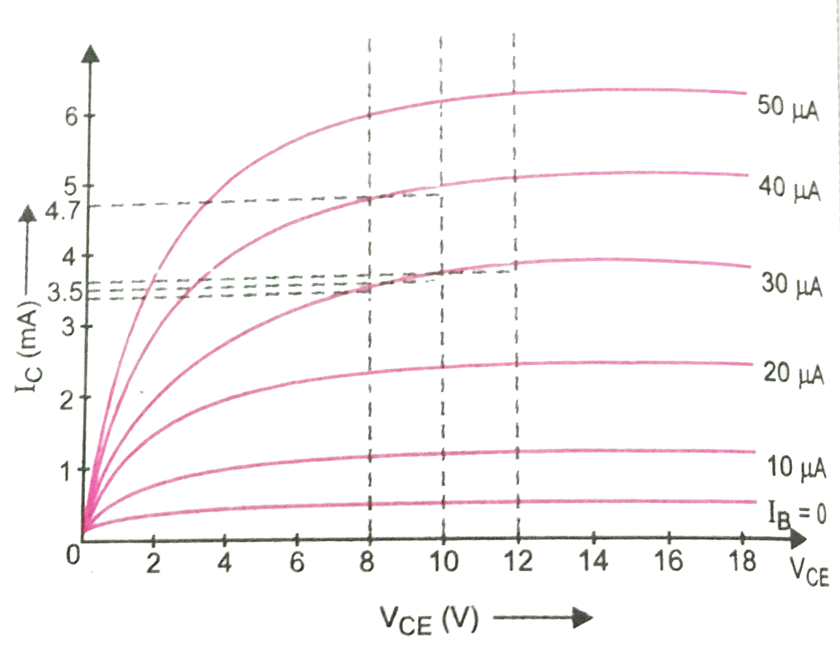
(i) dynamic output resistance (ii) dc current gain and (iii) ac current gain at an opererating point `V_(CE)=10V`, when `I_(B)=30muA`.
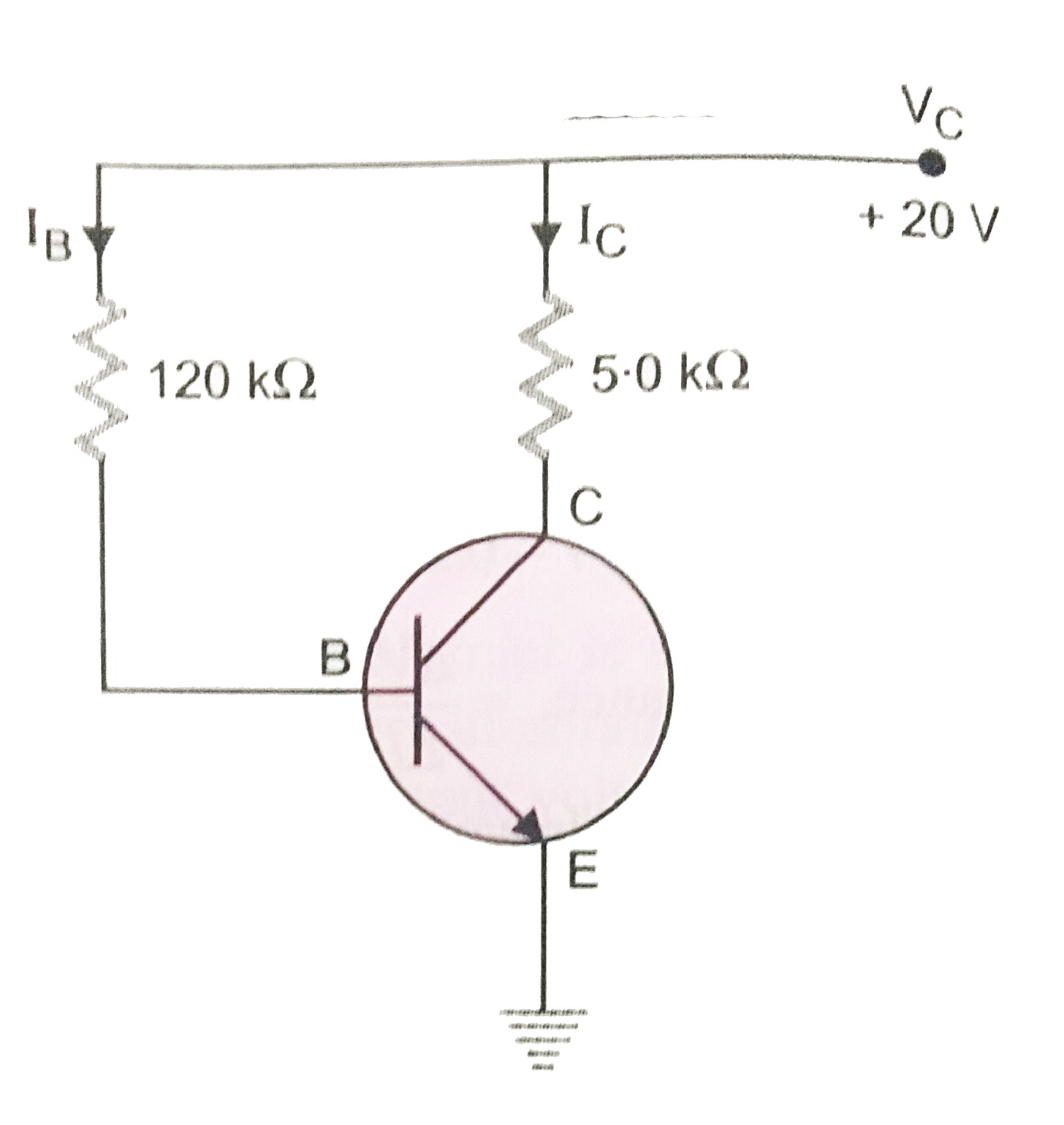
View SolutionIn the circuit Fig. the value of beta is 200. Find `I_(B), V_(CE), V_(BE)` and `V_(BC)`, when `I_(C)=2.5mA`. The transistor is in active, cut off or saturation state.
View SolutionIn the circuit shown in fig., the base current `I_(B)` is `10muA` and the collector current is `5.2mA`. (a) Can this transistor circuit be used as an amplifier? (b) What happen if the resistance `R_(C)` is `500Omega` and `I_(B), I_(C)` and `R_(B)` remain same as above?
View SolutionIn the circuit shown in Fig.
if we assume that when the input voltage at the base resistance is `5V, V_(BE)` is zero and `V_(CE)` is also zero. What is `I_,I_` and beta?
When the input is zero, then `I_` is zero. What would be the output wave form if the input wave form is as shown in Fig.
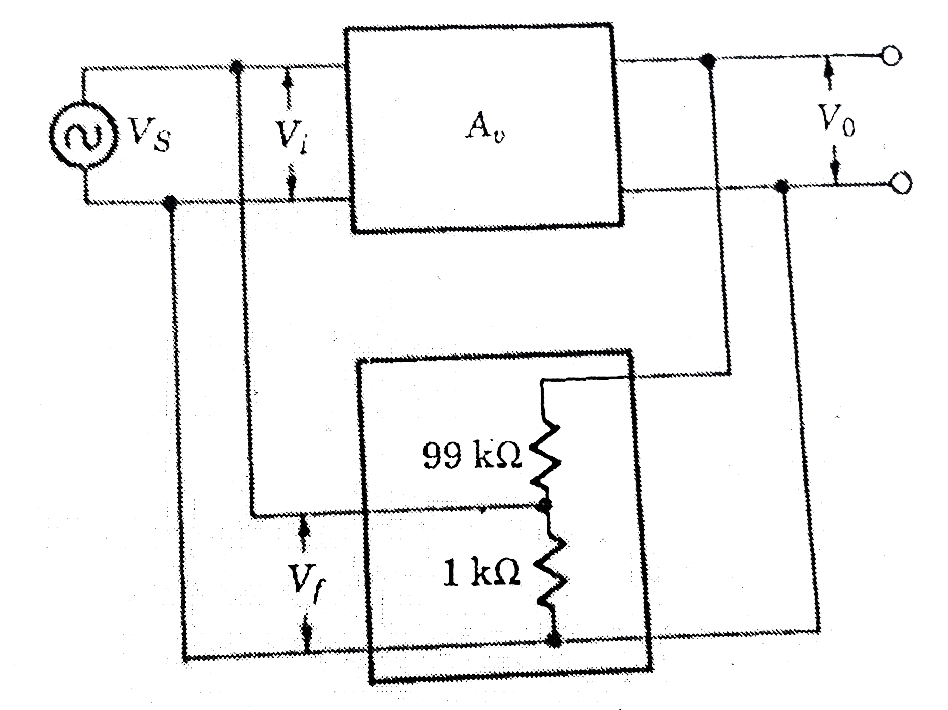
View SolutionAn amplifier is represented by the adjoining circuit . `r_(i)` is the input resistance of the amplifier and the voltage `v_(i)` is appearing across it. This voltage is amplified by a factor of `A_(v)` and apears across the load as voltage `v_(0)`.
View SolutionFig represents an amplifier circuit with an input internal resistance `r_(i)=50kOmega`. It is connected to an ac voltage source through a series resistor of `100kOmega`. The no load voltage gain of the transistor is 100. What is the apparent gain of the amplifier?
View SolutionIn the circuit, shown in fig `v_(s)=0.2V, v_(0)=-10V`. Find `v_(i)` and gain `A_(v)=v_(0)//v_(i)` and `A_(v)^(')=v_(0)/v_(s)`?
View SolutionPerform binary addition on the following sets numbers.
(a) 110010 and 111101 (b) 101010 and 010101 (c) 111111 and 000001
View SolutionComplement `(1's)` the following binary numbers.
(a) 110010 (b) 111101 (c) 101010 (d) 111111
View SolutionFind the `2's` complement of the following numbers?
(a) 111111 (b)000000 (c) 101010 (d) 001001
View SolutionPerform subtraction on the following sets of numbers.
(a) 110010 and 111101 (b) 010101 and 101010 (c) 1000001 and1111111
View SolutionWrite the output waveform of the OR gate for the inputs
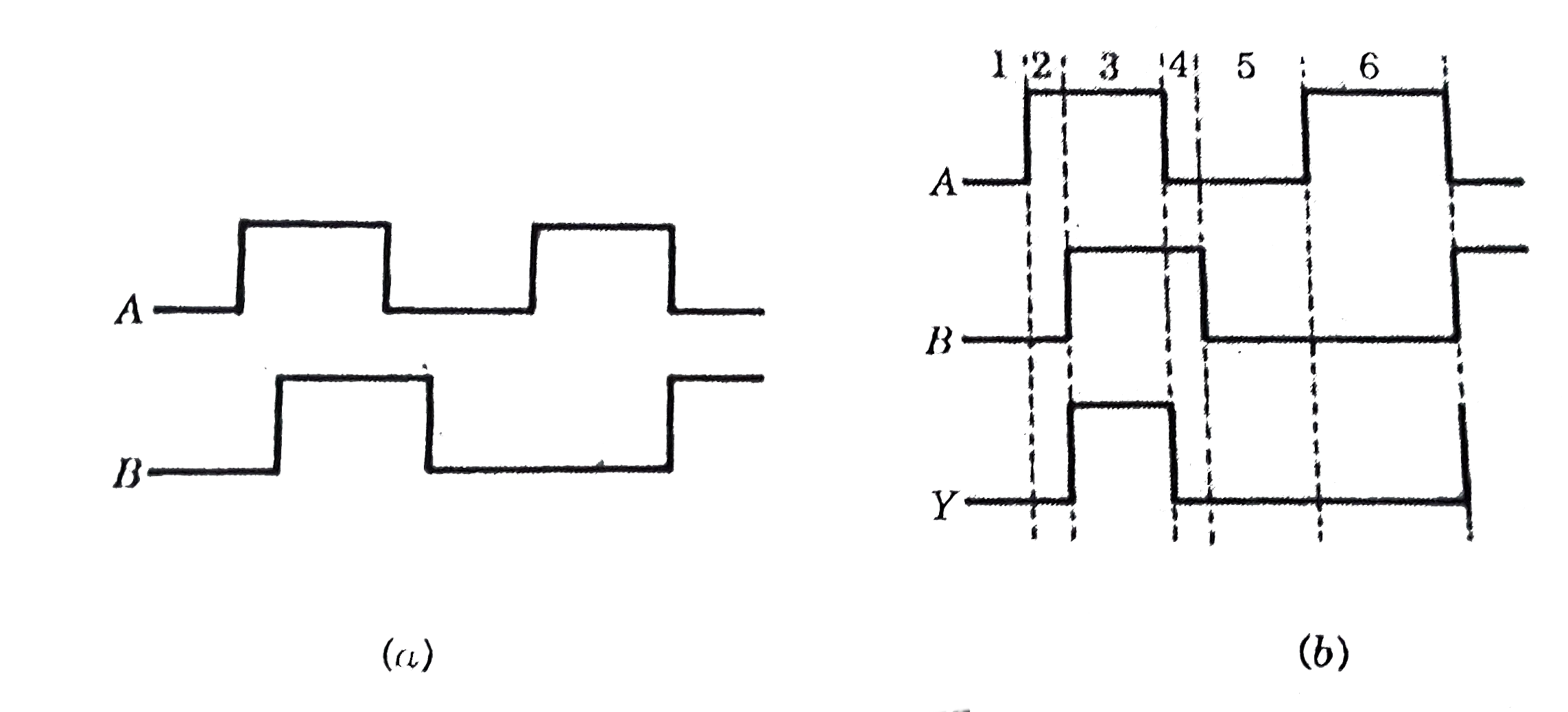
View SolutionTwo input waveforms `A` and `B` shown in fig (a) are applied to an AND gate.Write the output waveform.
View SolutionWrite the output waveform for the gates
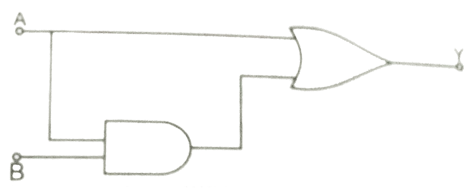
View SolutionWrite the Boolean equation and the truth table for the circuit shown in fig. What will be the output if both inputs are high?
View SolutionExpress by a truth table, the output Y for all possible input A and B in the following circuit Fig.
View SolutionThe output of an OR gate is connected to both the input of a NOR gate. Draw the logic circuit of the combination and write the truth table.
View SolutionThe output of and AND gate is connected to both the inputsof a NAND gate. Draw the logic circuit of this combinationn of gates and write its truth table.
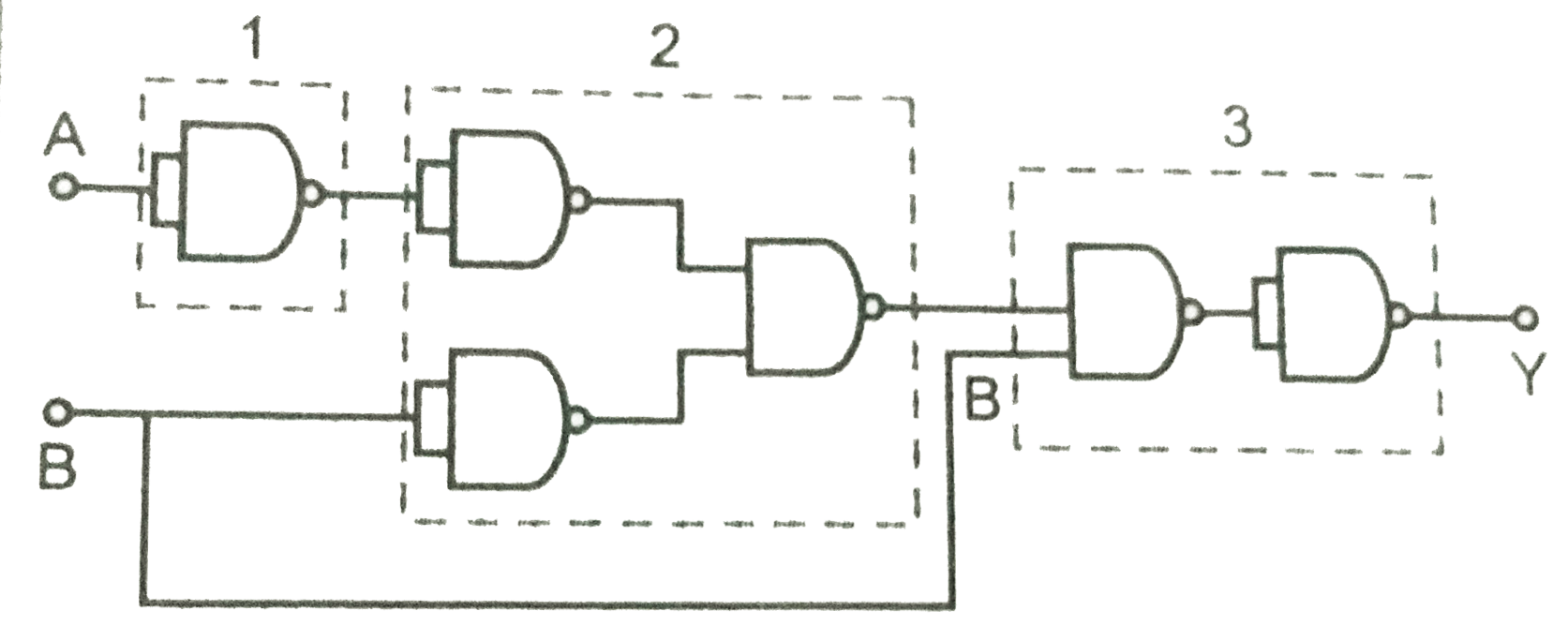
View SolutionIdentify which basic gate, OR, AND and NOT is represented by the circuits in the dotted line boxes 1, 2 and 3 Fig.
View SolutionWrite the truth table for the circuit shown in fig. Show that it represents a XOR gate.

View SolutionWrite the Boolean equation and the truth table for the circuit shown in fig. Which input words does the circuit recognise?
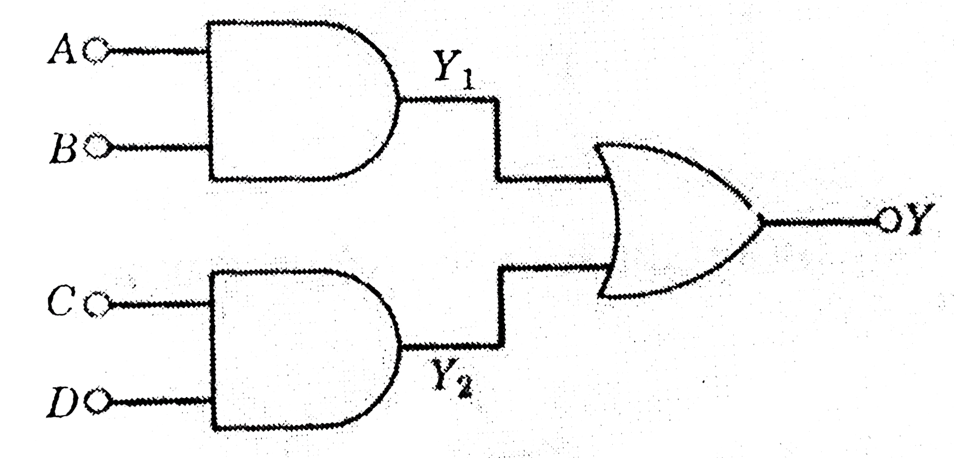
View Solution
ILLUSTRATION_TYPE questions and complete solutions for chapter SOLIDS AND SEMICONDUCTOR DEVICES of DHANPAT RAI & CO PHYSICS (HINGLISH) of Class 12