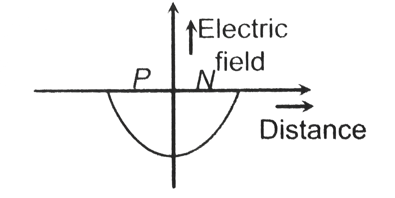
In the middle of the depletion layer of a reverse - biased p−n junction , the
A
Potential is zero
B
Electric field is zero
C
Potential is maximum
D
Electric field is maximum
Video Solution
Text Solution
The correct Answer is:D
The electric field strength versus distance curve across the P−N junction is as follows

Barrier potential of a P−N junction diode does not depends on
|
Topper's Solved these Questions
- SEMICONDUCTOR ELECTRONICSBOOK - A2ZCHAPTER - SEMICONDUCTOR ELECTRONICSEXERCISE - Diode In Circuits
40 Videos
- SEMICONDUCTOR ELECTRONICSBOOK - A2ZCHAPTER - SEMICONDUCTOR ELECTRONICSEXERCISE - Junction Transistor
47 Videos
- SEMICONDUCTOR ELECTRONICSBOOK - A2ZCHAPTER - SEMICONDUCTOR ELECTRONICSEXERCISE - Classification Of Metals
64 Videos
- NUCLEAR PHYSICSBOOK - A2ZCHAPTER - NUCLEAR PHYSICSEXERCISE - Section D - Chapter End Test
29 Videos
- SOURCE AND EFFECT OF MAGNETIC FIELDBOOK - A2ZCHAPTER - SOURCE AND EFFECT OF MAGNETIC FIELDEXERCISE - Section D - Chapter End Test
30 Videos
Similar Questions
Knowledge Check
The n-side of the depletion layer of a p-n junction :
Aalways has same width as of the p-side.Bhas no bound charges.Cis negatively charged.Dis positively charged.In the depletion region of an unbiased p-n junction diode there are
AOnly electronsBOnly fixed ionsCOnly holesDBoth electrons and holesIn the depletion region of the an unbaised p-n junction diode, there are
Aonly free electrons.Bonly holes.Cboth electrons and holes.Donly immobile charged ions.
Explain the formation of depletion layer and potential barier in a p-n junction.
View SolutionDefine the terms 'depletion layer and barrier potential' for a p-n junction. How does (i) an increase in the doping concentration, and (ii) biasing across the junction, affect the width of the depletion layer ?
View SolutionWhich of the following shows a reverse biased p-n junction diode ?
View SolutionThe reverse biasing in a p-n junction diode
View SolutionThe reverse biasing in a PN junction diode
View Solution
