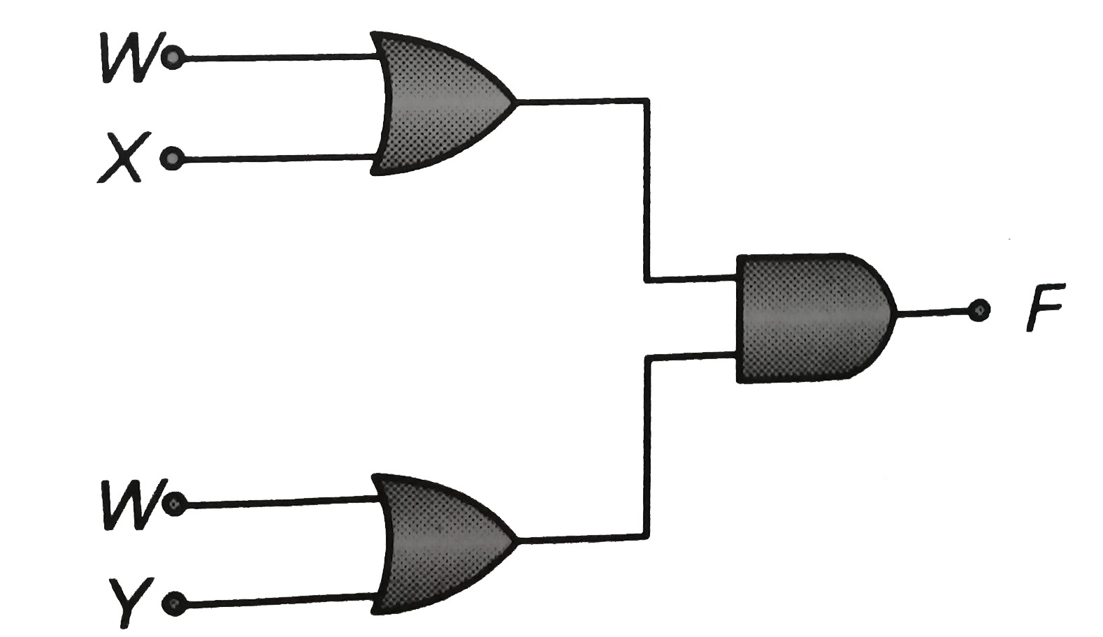
The diagram of a logic circuit is given below. The output F of the circuit is represented by

A
W.(X+Y)
B
W.(X.Y)
C
W+(X.Y)
D
W+(X+Y)
Video Solution
Text Solution
The correct Answer is:C
Output of upper OR gate=W+X
Output of lower OR gate =W+Y
Net output F=(W+X)(W+Y)
=WW+WY+XW+XY (Since WW=W)
=W(1+Y)+XW+XY (Since 1+Y=1)
=W+XW+XY=W(1+W)+XY=W+XY
|
Topper's Solved these Questions
- SEMICONDUCTOR ELECTRONICSBOOK - A2ZCHAPTER - SEMICONDUCTOR ELECTRONICSEXERCISE - Problems Based On Mixed Concepts
32 Videos
- SEMICONDUCTOR ELECTRONICSBOOK - A2ZCHAPTER - SEMICONDUCTOR ELECTRONICSEXERCISE - Section B - Assertion Reasoning
22 Videos
- SEMICONDUCTOR ELECTRONICSBOOK - A2ZCHAPTER - SEMICONDUCTOR ELECTRONICSEXERCISE - Junction Transistor
47 Videos
- NUCLEAR PHYSICSBOOK - A2ZCHAPTER - NUCLEAR PHYSICSEXERCISE - Section D - Chapter End Test
29 Videos
- SOURCE AND EFFECT OF MAGNETIC FIELDBOOK - A2ZCHAPTER - SOURCE AND EFFECT OF MAGNETIC FIELDEXERCISE - Section D - Chapter End Test
30 Videos
Similar Questions
Knowledge Check
The output for the given, circuit is
 A(A+B)⋅¯¯¯BB(A⋅B)⋅¯¯¯BC(A+B)⋅BD(A⋅B)⋅B
The ouput Y of the logic circuit given below is
 AA+BB¯¯¯AC¯¯¯¯¯¯¯¯¯¯¯¯¯¯A−B¯¯¯AD¯¯¯¯¯¯¯¯¯¯¯¯¯¯A−BA
The output of the given circuit in Figure
 Awould be zero at all times.Bwould be like a half wave rectifier with positive cycles in output.Cwould be like a half wave rectifier with negative cycles in output.Dwould be like that of a full wave rectifier.


