In a p−n junction
A
P and N both are at same potential
B
High potential at N side and low potential at P side
C
High potential P side and low potential at N side
D
Low potential at N side and zero potential at P side
Video Solution
Text Solution
The correct Answer is:B
For conduction, p−n junction must be forward biased. For this p-side should be connected to higher potential and n-side to lower potential.
|
Topper's Solved these Questions
- SEMICONDUCTOR ELECTRONICSBOOK - A2ZCHAPTER - SEMICONDUCTOR ELECTRONICSEXERCISE - AIIMS Questions
38 Videos
- SEMICONDUCTOR ELECTRONICSBOOK - A2ZCHAPTER - SEMICONDUCTOR ELECTRONICSEXERCISE - Assertion Reason
18 Videos
- SEMICONDUCTOR ELECTRONICSBOOK - A2ZCHAPTER - SEMICONDUCTOR ELECTRONICSEXERCISE - Section B - Assertion Reasoning
22 Videos
- NUCLEAR PHYSICSBOOK - A2ZCHAPTER - NUCLEAR PHYSICSEXERCISE - Section D - Chapter End Test
29 Videos
- SOURCE AND EFFECT OF MAGNETIC FIELDBOOK - A2ZCHAPTER - SOURCE AND EFFECT OF MAGNETIC FIELDEXERCISE - Section D - Chapter End Test
30 Videos
Similar Questions
Knowledge Check
What happens to the depletion region of a p-n junction ?
ADecreases if reverse biasedBIncreases if reverse biasedCIncreases if forward biasedDRemains the same in reverse and forward biasingWhen a p-n junction diode is reverse biased
Aelectrons and holes are attracted towards each other and move towards the depletion region.Belectrons and holes move away form the deplection region.Cheight of the potential barrier decreasesDno change in the current takes placeThe depletion region of a p-n junction contains :-
Aelectrons onlyBelectrons and holes bothCholes onlyDneither electrons nor holes
In p-n junction, p-side is known as........and n-side is known as..........
View SolutionWhen a p-n junction diode is reverse biased
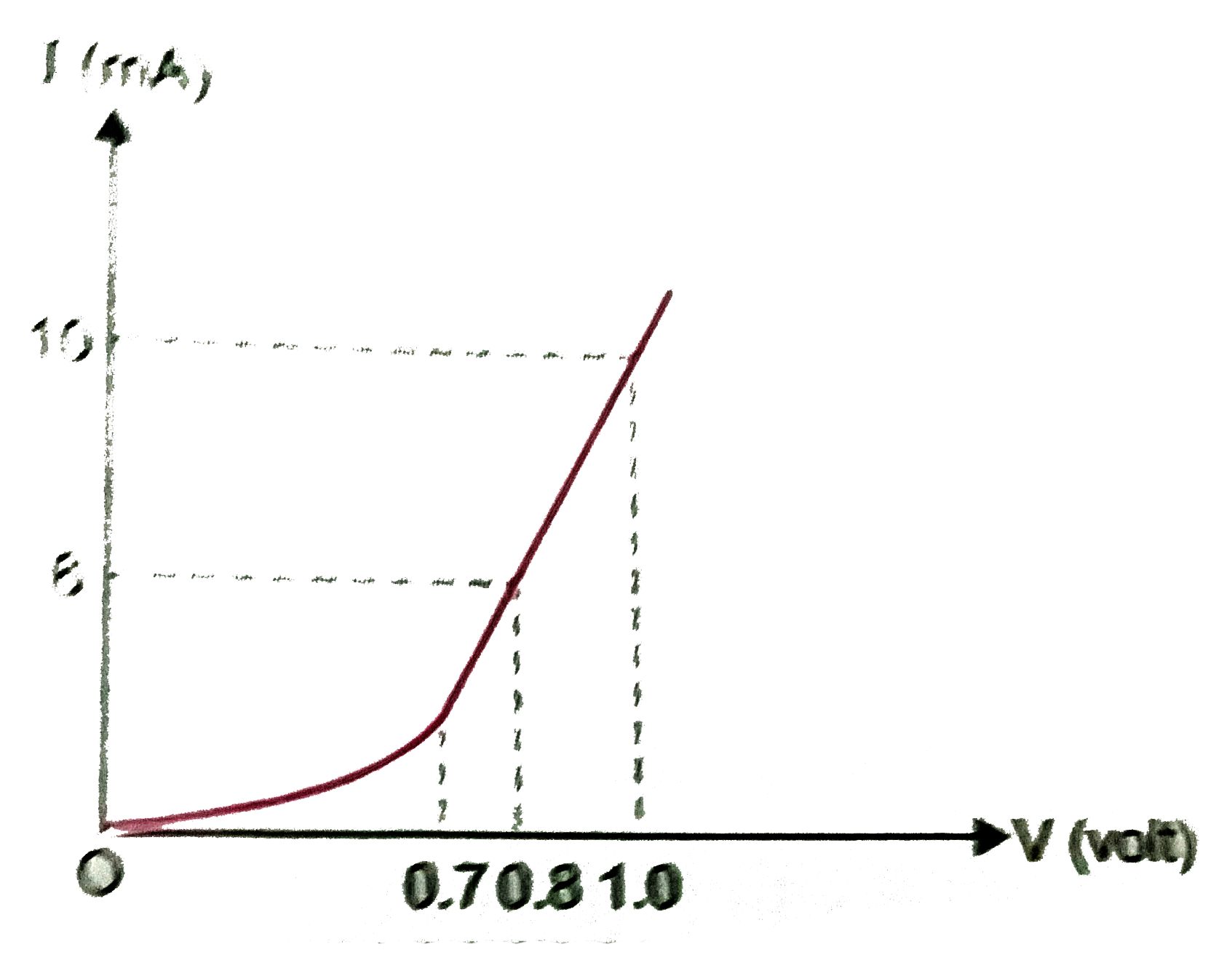
View SolutionThe forward characteristic of p-n junction is shown in Fig.What is the dynamical resistance of p-n junction at 0.9V?

View SolutionTo make a p-n junction conducting
View SolutionThe n-side of the depletion layer of a p-n junction :
View Solution
