Dicuss how the OR gate is realised from the NAND gate.
Video Solution
Text Solution
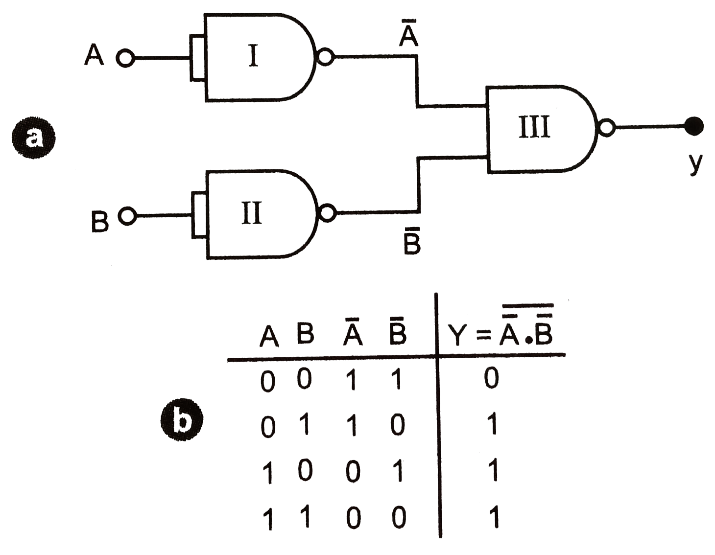
If the input terminals of NAND gate are joined togather we get NOT gate. Now if the input A and B are inverted by using two NOT gates (obtained from NAND gates) and their outputs are jointly fed to the NAND gate as shown in Fig.9.35, we get the arrangement which works as OR gate.

Explaination. The output of gate I is,
y1=¯¯¯¯¯¯¯¯A.A=¯¯¯A+¯¯¯A=¯¯¯A
The output of gate II is,
y2=¯¯¯¯¯¯¯¯B.B=¯¯¯B+¯¯¯B=¯¯¯B
The output of gate III is,
y=¯¯¯¯¯¯¯¯¯y1.y2=¯¯¯¯¯¯¯¯¯¯¯¯A.¯¯¯B=¯¯¯¯¯¯¯A+¯¯¯¯¯¯B=A+B
As y=A+B, is the Boolean expression for OR gate, thus the combination works as OR gate. The truth table of the arrangement is shown in.
|
Updated on:21/07/2023
Topper's Solved these Questions
- BOOK - PRADEEPCHAPTER - ELECTRONIC DEVICESEXERCISE - SAMPLE PROBLEM2videos
ELECTRONIC DEVICES
- BOOK - PRADEEPCHAPTER - ELECTRONIC DEVICESEXERCISE - CONCEPTUAL PROBLEMS1videos
ELECTRONIC DEVICES
- BOOK - PRADEEPCHAPTER - ELECTROMAGNETIC WAVESEXERCISE - II Focus multiple choice question5videos
ELECTROMAGNETIC WAVES
- BOOK - PRADEEPCHAPTER - ELECTROSTATICSEXERCISE - ASSERTION-REASON TYPE QUESTIONS2videos
ELECTROSTATICS
Similar Questions
Knowledge Check
- Question 1 - Select One
NAND gate is-
Aa basic gateBnot a universal gateCa universal gateDa universal gate - Question 2 - Select One
How many NOR gates are used to form an AND gate
A1B2C3D4 - Question 3 - Select One
How many NAND gate are used to from AND gate?
A1B2C3D4

