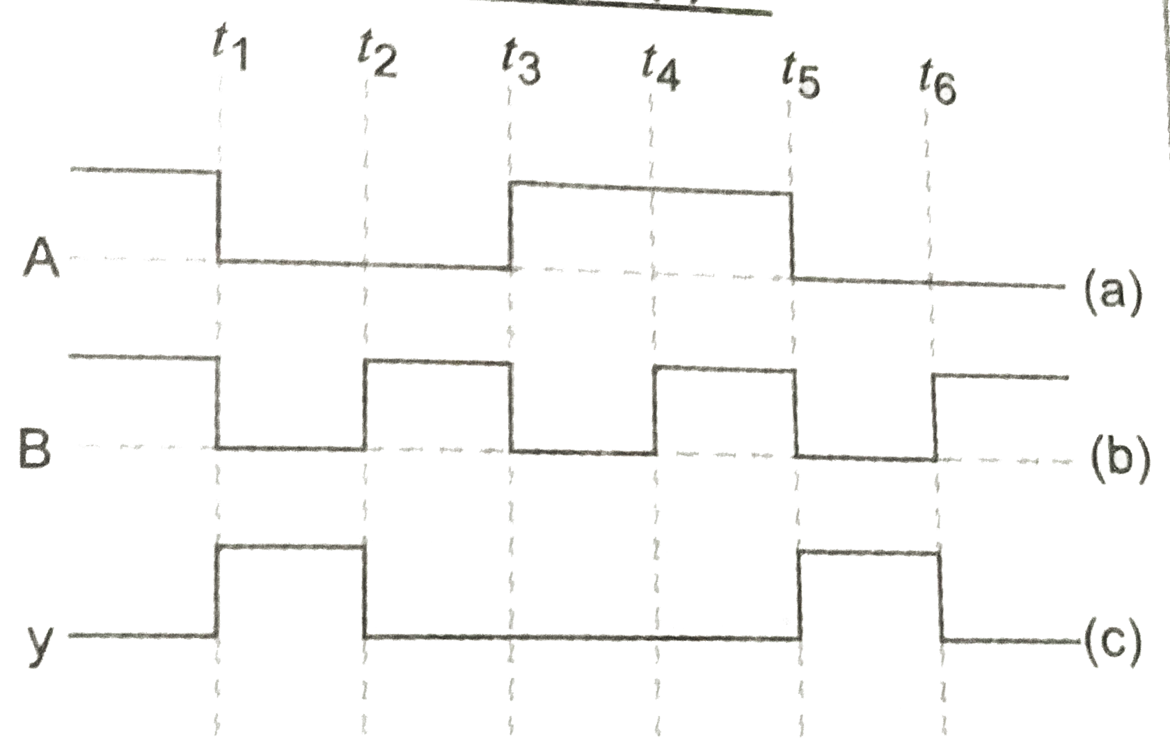
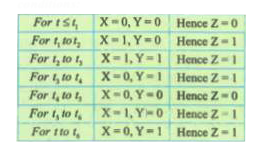
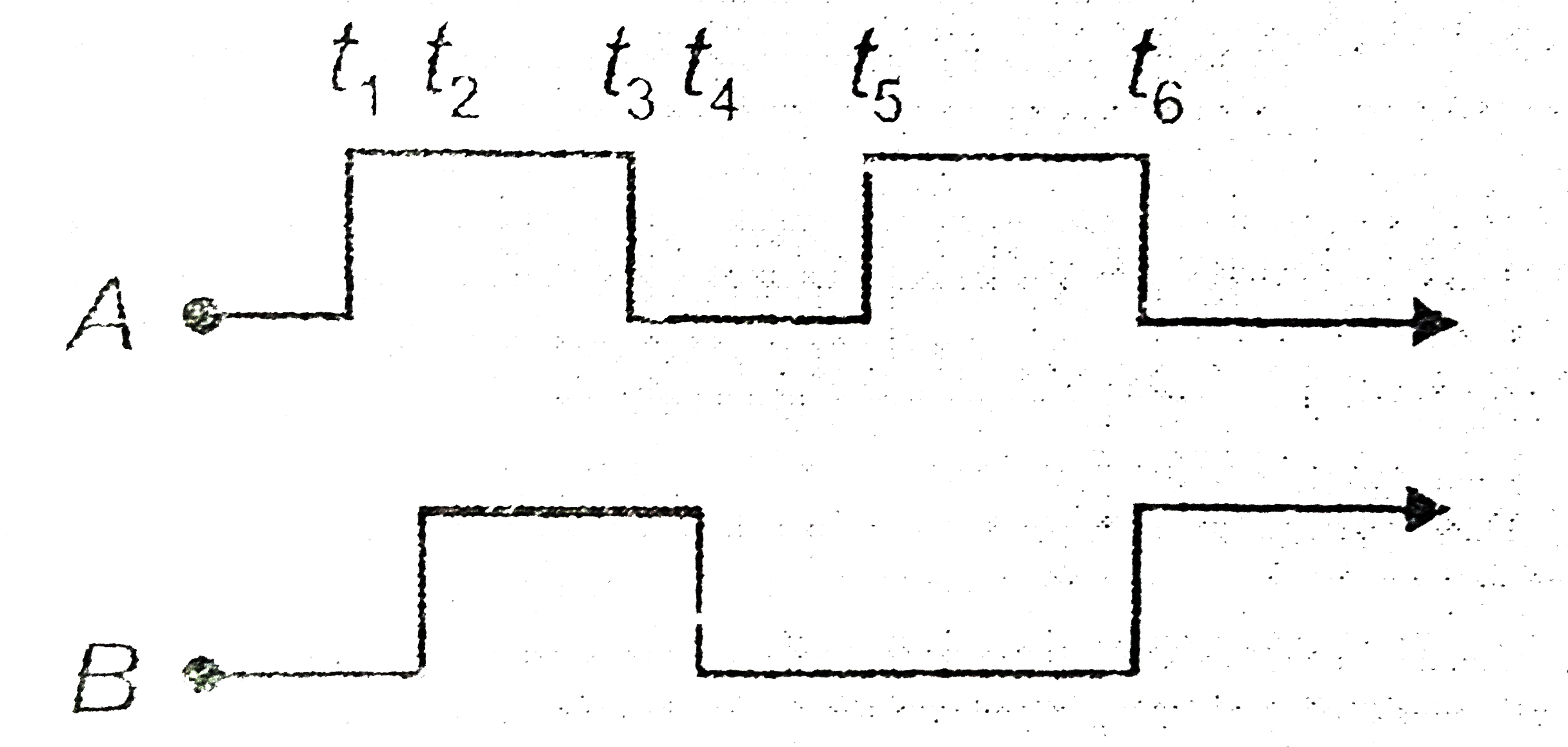
Sketch the output Y from NAND gate having input A A and B given below, Fig.
To solve the problem of sketching the output Y from a NAND gate with inputs A and B, we will follow these steps:
Step 1: Understand the NAND Gate
The NAND gate is a digital logic gate that outputs false or 0 only when both of its inputs are true or 1. The Boolean expression for a NAND gate is given by:
\( Y = (A \cdot B)' \)
This means that the output Y is the negation (NOT) of the AND of inputs A and B.
Step 2: Identify Input Values
From the problem, we have two inputs A and B. Let's assume the values of A and B are as follows:
- Input A: 1, 0, 0, 1, 1, 0, 0 (in sequence)
- Input B: 1, 0, 1, 0, 1, 0, 1 (in sequence)
Step 3: Create a Truth Table
We will create a truth table to evaluate the output Y based on the inputs A and B.
| A | B | A · B | Y = (A · B)' |
|---|---|-------|--------------|
| 1 | 1 | 1 | 0 |
| 0 | 0 | 0 | 1 |
| 0 | 1 | 0 | 1 |
| 1 | 0 | 0 | 1 |
| 1 | 1 | 1 | 0 |
| 0 | 0 | 0 | 1 |
| 0 | 1 | 0 | 1 |
Step 4: Determine the Output Values
From the truth table, we can derive the output values for Y based on the inputs A and B:
- For (1, 1) → Y = 0
- For (0, 0) → Y = 1
- For (0, 1) → Y = 1
- For (1, 0) → Y = 1
- For (1, 1) → Y = 0
- For (0, 0) → Y = 1
- For (0, 1) → Y = 1
Thus, the output sequence for Y is:
0, 1, 1, 1, 0, 1, 1
Step 5: Sketch the Output Waveform
Now, we will sketch the output waveform based on the output values derived:
- Start at 0 (bottom line)
- Go to 1 (top line) for the first 1
- Return to 0 for the next 0
- Stay at 1 for the next three 1s
- Return to 0 for the next 0
- Go back to 1 for the last two 1s
The waveform will look like this:
Y:_____|⌊|⌊⌊|⌊||0−−−||||∣|||⊢−Time01234567
The NAND gate is a digital logic gate that outputs false or 0 only when both of its inputs are true or 1. The Boolean expression for a NAND gate is given by:
\( Y = (A \cdot B)' \)
This means that the output Y is the negation (NOT) of the AND of inputs A and B.
From the problem, we have two inputs A and B. Let's assume the values of A and B are as follows:
- Input A: 1, 0, 0, 1, 1, 0, 0 (in sequence)
- Input B: 1, 0, 1, 0, 1, 0, 1 (in sequence)
We will create a truth table to evaluate the output Y based on the inputs A and B.
|---|---|-------|--------------|
| 1 | 1 | 1 | 0 |
| 0 | 0 | 0 | 1 |
| 0 | 1 | 0 | 1 |
| 1 | 0 | 0 | 1 |
| 1 | 1 | 1 | 0 |
| 0 | 0 | 0 | 1 |
| 0 | 1 | 0 | 1 |
From the truth table, we can derive the output values for Y based on the inputs A and B:
- For (1, 1) → Y = 0
- For (0, 0) → Y = 1
- For (0, 1) → Y = 1
- For (1, 0) → Y = 1
- For (1, 1) → Y = 0
- For (0, 0) → Y = 1
- For (0, 1) → Y = 1
0, 1, 1, 1, 0, 1, 1
Now, we will sketch the output waveform based on the output values derived:
- Start at 0 (bottom line)
- Go to 1 (top line) for the first 1
- Return to 0 for the next 0
- Stay at 1 for the next three 1s
- Return to 0 for the next 0
- Go back to 1 for the last two 1s
Y:_____|⌊|⌊⌊|⌊||0−−−||||∣|||⊢−Time01234567
Topper's Solved these Questions
- BOOK - PRADEEPCHAPTER - ELECTRONIC DEVICESEXERCISE - SAMPLE PROBLEM2videos
ELECTRONIC DEVICES
- BOOK - PRADEEPCHAPTER - ELECTRONIC DEVICESEXERCISE - CONCEPTUAL PROBLEMS1videos
ELECTRONIC DEVICES
- BOOK - PRADEEPCHAPTER - ELECTROMAGNETIC WAVESEXERCISE - II Focus multiple choice question5videos
ELECTROMAGNETIC WAVES
- BOOK - PRADEEPCHAPTER - ELECTROSTATICSEXERCISE - ASSERTION-REASON TYPE QUESTIONS2videos
ELECTROSTATICS
Similar Questions
Knowledge Check
- Question 1 - Select One
The output of NAND gate is 0 :
AIf both input are 0BIf one input is 0 and the other input is 1CIf both input are 1DEither if both input are 1 or if one of the inputs is 1 and the other is 0 - Question 2 - Select One
The output of NAND gate is 0 :
AIf both input are 0BIf one input is 0 and the other input is 1CIf both input are 1DEither if both input are 1 or if one of the inputs is 1 and the other is 0 - Question 3 - Select One
The output of a NAND gate is 0
AIf both inputs are zeroBIf one input is 0 and the other input is 1CIf both inputs are 1DEither if both inputs are 1 or if one of the inputs is 1 and the other 0
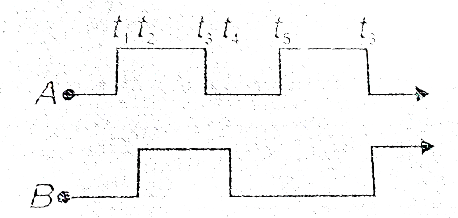
Sketch the output wavefrom Y from a NAND gate having following inputs A and B
 View Solution
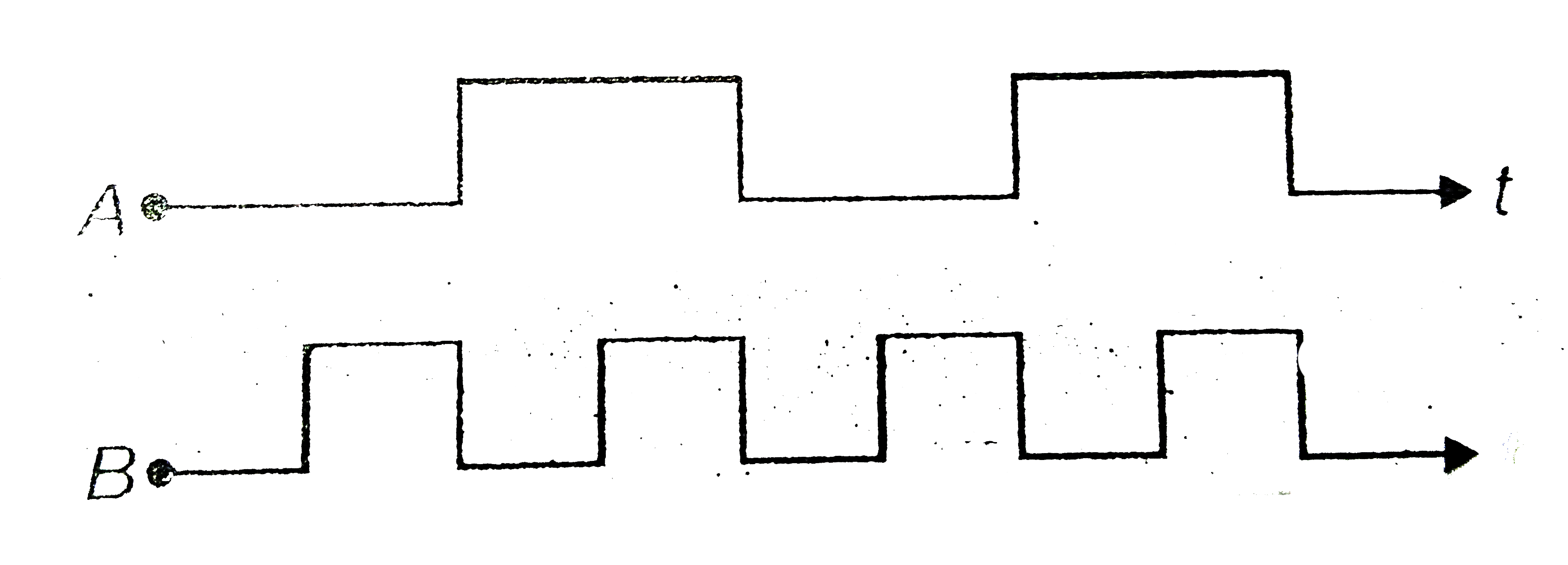
Sketch the output waveform Y from a NAND gate having following inputs A and B
 View Solution
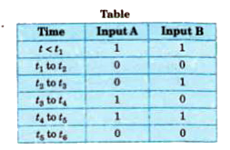
Sketch inputs A,B and output Y from a NAND gate from the table given below
 View Solution
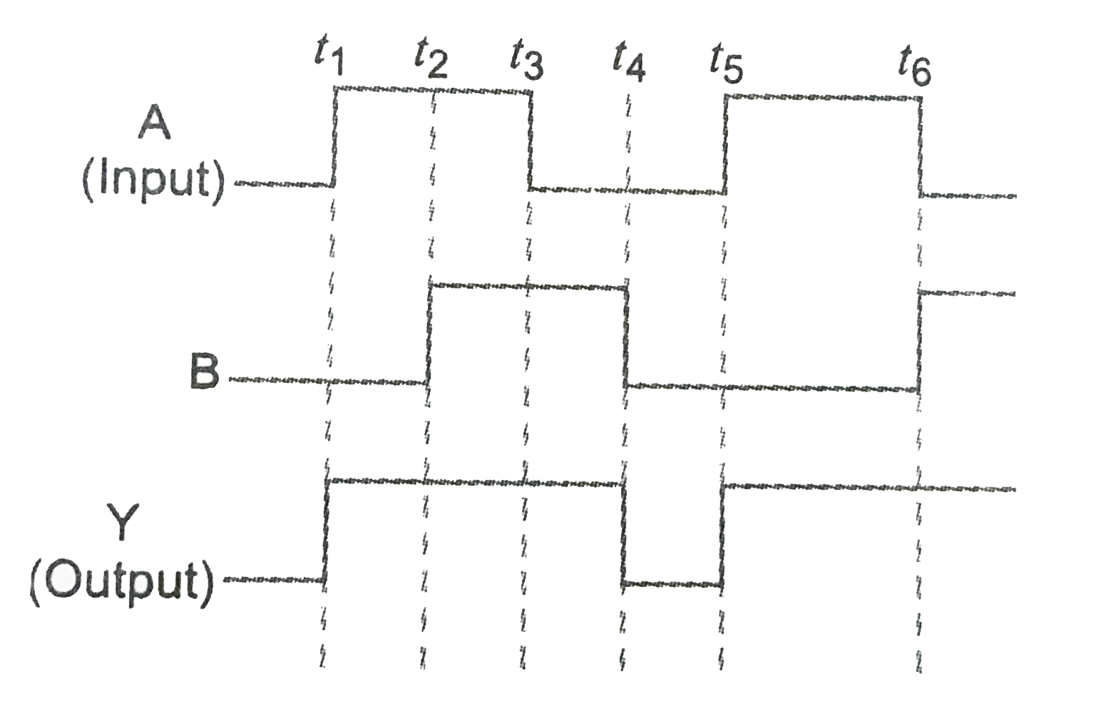
Justify the output wavefrom (y) of the OR gate for input and as gives in Fig.
 View Solution
Sketch the output waveform obtained from AND gate for the following inputs A and B.
 View Solution


