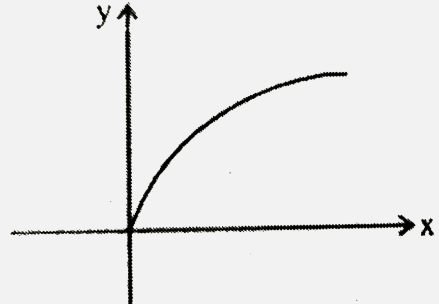
Draw the typical input and output characteristics of an n-p-n transistor in CE configuration. Show how these characteristics can be used to determine (a) the input resistance (ri) and (b) current amplification factor (β).Solution in Bengali
Step by step video & image solution for Draw the typical input and output characteristics of an n-p-n transistor in CE configuration. Show how these characteristics can be used to determine (a) the input resistance (r_(i)) and (b) current amplification factor (beta). by Physics experts to help you in doubts & scoring excellent marks in Class 12 exams.
Topper's Solved these Questions
Similar Questions
Consider the junction diode as ideal. The value of current flowing through AB is
 09:34View Solution
For the same angle of incidence, the angles of refraction in three different media A, B and C are15∘,25∘ and 35∘ respectively. In which medium, will the velocity of light be minimum ?
02:16View SolutionDraw a circuit diagram of a transistor amplifier in CE configuration. Define the terms (i) Input resistance and (ii) Current amplification factor. How are these determined using input and output characteristics?
11:56View SolutionWhich is correct for the graph ?
 04:46View Solution
Draw typical output characteristics of an n-p-n transistor in CE configuration. Show how these characteristics can be used to determine output resistance.
06:12View SolutionShow the circuit arrangement for studying the input and output characteristics of a n-p-n transistor in CE configuration.
View SolutionOutline the method of drawing input and output characteristics with a neat labelled diagram of an N-P-N transistor in CE configuration.
View SolutionDraw circuit diagram for n-p-n transistor to draw input and output characteristics in common base configuration. Draw the input and ouput curves and explain them.
00:24View SolutionDraw a circuit diagram to study characteristics of n-p-n transistor in CE configuration. Draw the sketch of input and output characteristics of this configuration . Define current amplification factor ?
02:56View Solution(i) Draw a circuit diagram to study the input and output characteristics of an n-p-n transistor in its common emitter configuration. Draw the typical input and output characteristics.
(ii) Explain, with the hepl of a circuit diagram, the working of n-p-n transistor as a common emitter amplifier.03:02View Solution(a) Draw the circuit arrangement for studying the input and output characteristics of an n-p-n transistor in CE configuration . With the help of these characteristics define (i) input resistance , (ii) current amplification factor . (b) Describe briefly with the help of a circuit diagram how an n-p-n transistor is used to produce self-sustained oscillations .
04:21View SolutionDraw typical output characteristics of an n-p-n transistor in CE configuration. Show how these characteristics can be used to determine output resistance.
04:36View SolutionDraw the diagram of the circuit arangement used for studying the 'input' and the 'output' characteristics of an n-p-n transistor inits CE configuration. Briefly explain how these two types of characteristics are obtained and draw these characteristics. (b) 'Define' the terms (i) Input resistance, (ii) Output resistance , (iii) Current amplification factor, for a given transistor.
03:18View Solution(i) Write the functions of three segments of a transistor. (ii) Draw the ciruit diagram or studying the input and output characteristics of n-p-n transisfor in common emitter configuration . Using the circuit explain how input characteristics are obtained .
View SolutionDraw the typical input and output characterisitics of an n-p-n transistor in CE configurtion . Show how these characteristic can be used to determine (a) the input resistance (r_(1)) and (b) current amplification factor (beta) .
08:35View Solution

