The minimum potential difference between the base and emitter required to switch a silicon transistor ON is approximately?
1V
3 V
5 V
4.2 V
The correct Answer is:A
Step by step video, text & image solution for The minimum potential difference between the base and emitter required to switch a silicon transistor ON is approximately? by Physics experts to help you in doubts & scoring excellent marks in Class 12 exams.
Topper's Solved these Questions
- BOOK - TARGET PUBLICATIONCHAPTER - SEMICONDUCTORSEXERCISE - Evaluation Test17videos
SEMICONDUCTORS
- BOOK - TARGET PUBLICATIONCHAPTER - SEMICONDUCTORSEXERCISE - Critical thinking32videos
SEMICONDUCTORS
- BOOK - TARGET PUBLICATIONCHAPTER - ROTATIONAL MOTION EXERCISE - MCQ245videos
ROTATIONAL MOTION
- BOOK - TARGET PUBLICATIONCHAPTER - STATIONARY WAVESEXERCISE - EVALUATION TEST16videos
STATIONARY WAVES
Similar Questions
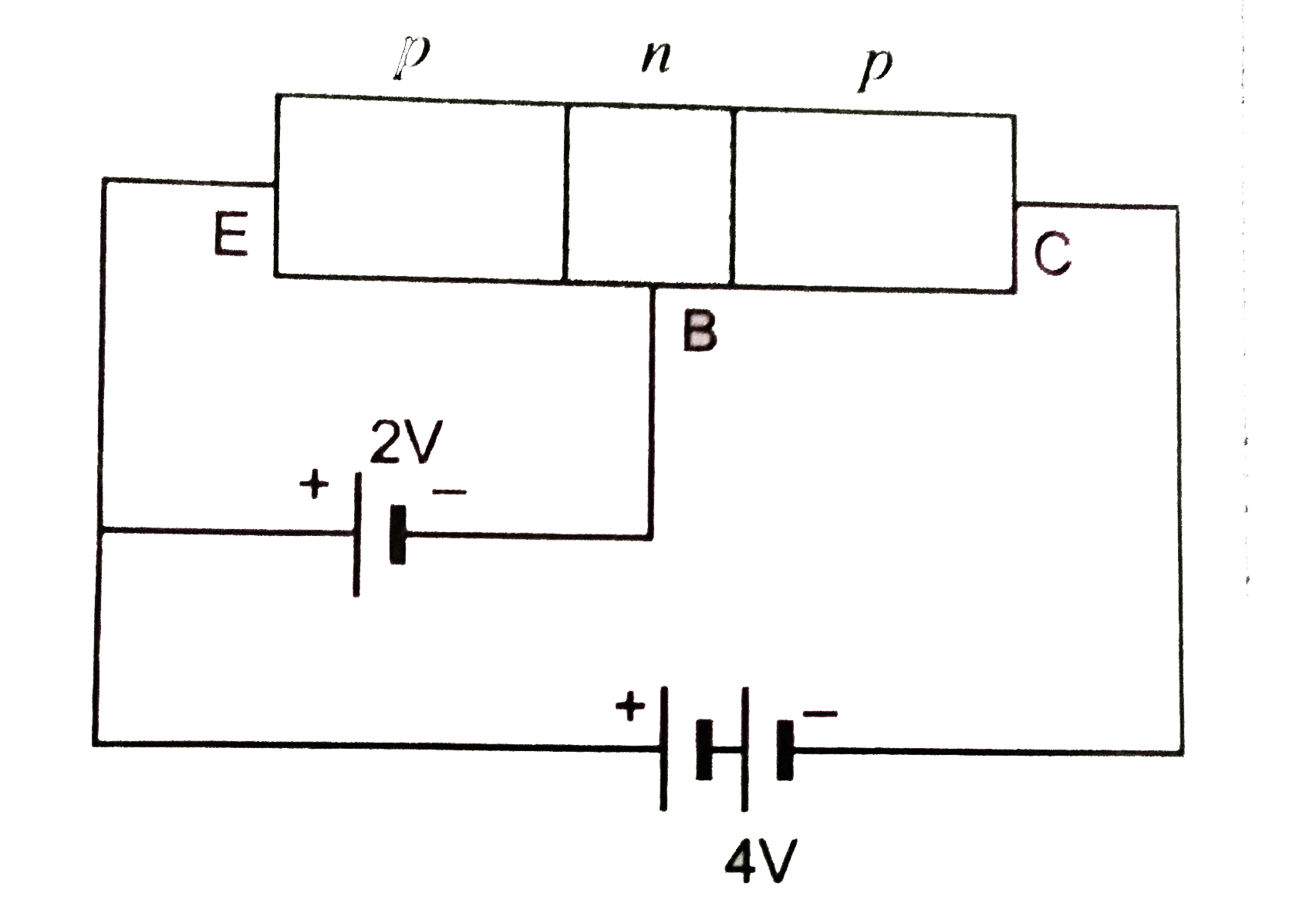
In the p-n-p transistor circuit shown in Fig.

What is the potential difference between base and collector?
What is the nature of biasing between emitter base junction and collector-base junction?View SolutionThe potential difference across the collector of a transistor, used in common emitter mode is 1.5V, with the collector resistance of 3kΩ. Find (i) the emitter current and (ii) the base current, if d.c. gain of the transistor is 50.
View Solution
Knowledge Check
- Question 1 - Select One
Minimum amount of energy required to remove a proton is approximately:
A2MeVB4 MeVC6 MeVD8 MeV - Question 2 - Select One
At the base emitter junction of a transistor one finds
Aforward biasBnarrow depletion layerClow resistanceDall the three (1, 2 and 3) - Question 3 - Select One
Emitter base and collector base junction in n-p-n transistor are
Aforward biased and reverse biased respectivelyBreverse biased and forward biased respectivelyCboth forward biasedDboth reverse biased
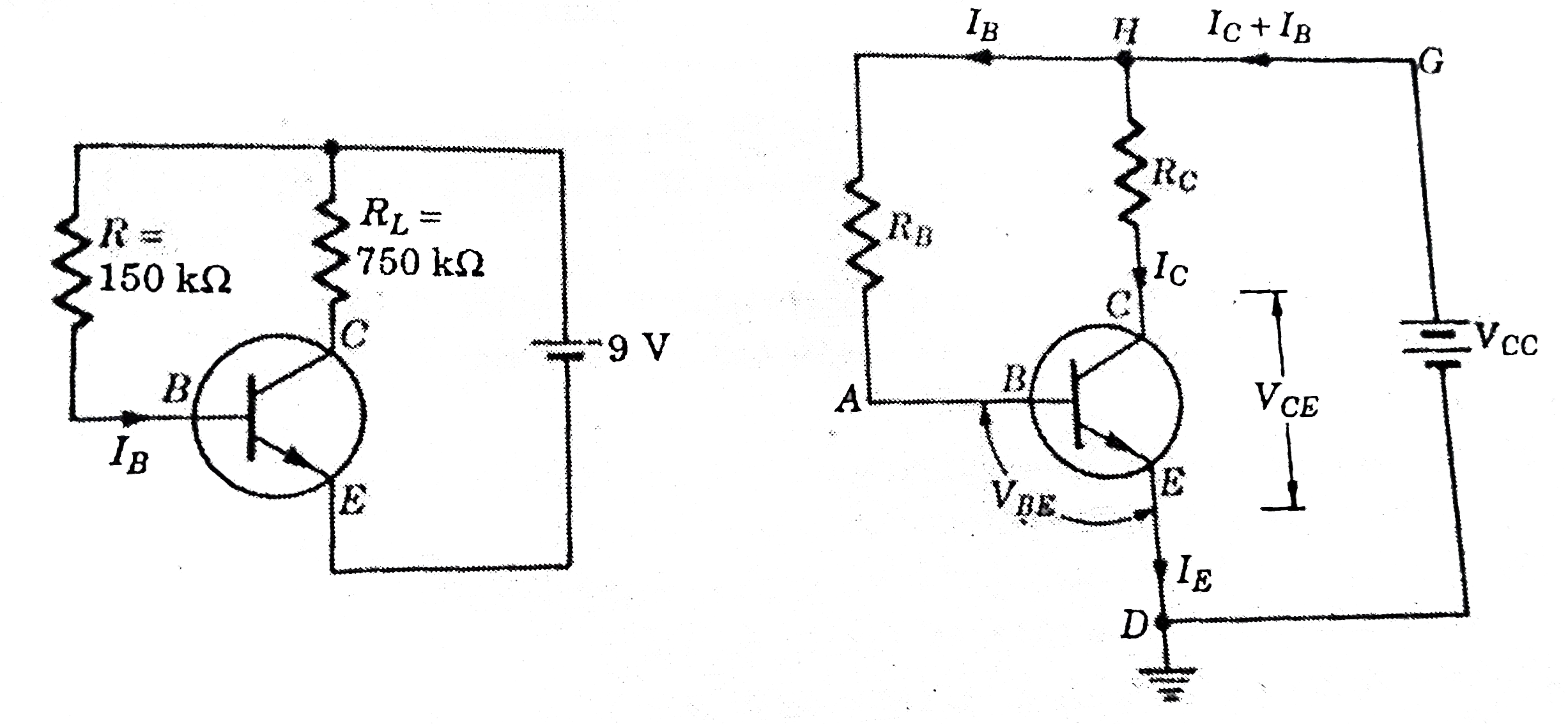
In a transistor circuit shown in fig, R has a resistance of 150kΩ,RL has a resistance of 750Ω, and the direct current gain of the transistor is 80. Assuming ther is negligible potential difference between B and E, calculate (a) the base current rent IB and (b) the potential difference betwen the collector and emitter.
 View Solution
How is the emitter base junction in the transistor biasing ?
View SolutionThe dc common emitter current gain of a n-p-n transistor is 50. The potential difference applied across the collector and emitter of a transistor used in CE configuration is, VCE=2V. If the collector resistance, RC=4Ω, the base current (IB) and the collector current (IC) are
View SolutionThe output characterstics of an n−p−n transistor represent, [IC = Collector current, VCE = potential difference between collector and emitter, IB = Base current, VBB = voltage given base , VBE = the potential difference between base and emitter].
View SolutionThe potential difference across the collector of a transistor, used in common emitter mode is 1.5 V, with the collector resistance of 3kΩ, the emitter current is [β−50]
View Solution

