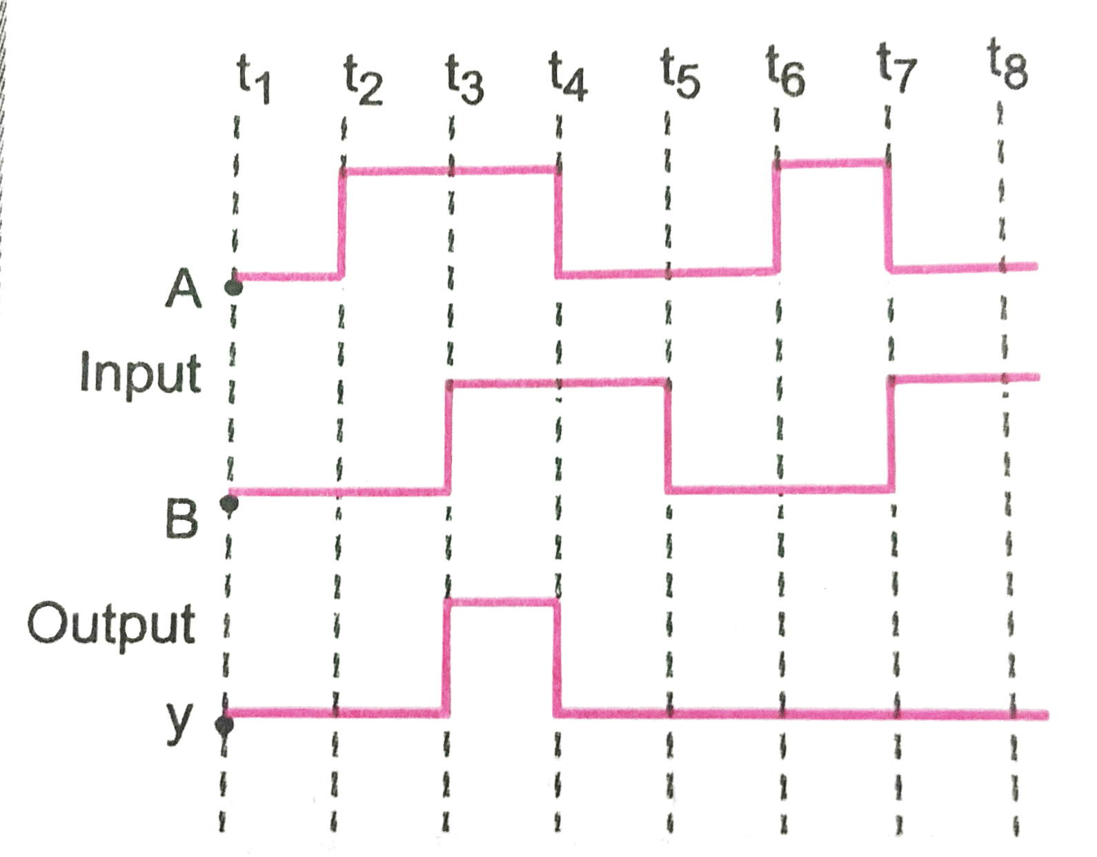
If the following waveform is applied to an OR gate, then write the output.
 Solution in Kannada
Output has the digital code 1 1 0 1 1 1 1 1 1 0
Topper's Solved these Questions
- BOOK - SUBHASH PUBLICATIONCHAPTER - SEMICONDUCTOR ELECTRONICSEXERCISE - FIVE MARKS QUESTIONS WITH ANSWERS9videos
SEMICONDUCTOR ELECTRONICS
- BOOK - SUBHASH PUBLICATIONCHAPTER - SEMICONDUCTOR ELECTRONICSEXERCISE - OPTIONAL NUMERICALS WITH SOLUTIONS6videos
SEMICONDUCTOR ELECTRONICS
- BOOK - SUBHASH PUBLICATIONCHAPTER - SEMICONDUCTOR ELECTRONICSEXERCISE - OPTIONAL NUMERICALS WITH SOLUTIONS6videos
SEMICONDUCTOR ELECTRONICS
- BOOK - SUBHASH PUBLICATIONCHAPTER - RAY OPTICS AND OPTICAL INSTRUMENTSEXERCISE - NUMERICALS WITH SOLUTIONS22videos
RAY OPTICS AND OPTICAL INSTRUMENTS
- BOOK - SUBHASH PUBLICATIONCHAPTER - SUPER MODEL QUESTION PAPER ( WITH ANSWERS ) EXERCISE - PART D26videos
SUPER MODEL QUESTION PAPER ( WITH ANSWERS )
Similar Questions
What is half wave rectification? Explain the working of a half wave rectifier. Indicate the waveforms of input and output voltage.
02:42View SolutionIf the peak value voltage in the secondary output ac voltage is 12V, then what will be the average DC in the case of HWR and FWR?
03:01View SolutionIf the peak value voltage in the secondary output ac voltage is 12V, then what will be the average DC in the case of HWR and FWR?
03:10View SolutionShow that lateral shift is equal to the thickness of the slab for grazing incidence.
02:13View SolutionDerive an expression for electrical conductivity.
View SolutionThe following Fig. shows the input waveforms (A,B) and the output waveform (y) of a gate. Identify the gate and write its truth table.
02:22View SolutionThe Fig.shows the input wavwforms A and B for 'AND' gate. Draw the output waveform and write the truth table for this logic gate.
 02:01View Solution
The Fig shown input waveforms A and B to a logic gate. Draw the output waveform for an OR gate. Write the truth table for this logic gate and draw its logic symbol.
 03:24View Solution
Write the output waveform of the OR gate for the inputs
02:36View SolutionWrite the output waveform for the gates
View SolutionShow the output waveform of OR gate for the following input waveforms of A and B
 05:33View Solution
show the output waveform of AND gate for the following input waveforms of A and B.
 02:45View Solution
Show the output waveform of OR gate for the following input waveforms of A and B
02:32View SolutionSketch the output waveform obtained from AND gate for the following inputs A and B.
 02:18View Solution
चित्र में एक गेट के निवेश तरंगरूप (A,B) और निर्गत तरंगरूप (Y ) दर्शाए गए हैं। गेट को पहचाने और इसकी सत्यमान सारणी लिखें।
01:59View Solution

