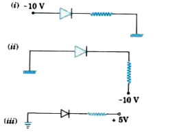
Write the value of resistance offered by an ideal diode when (i) forward biased (ii) reverse biased
To answer the question regarding the resistance offered by an ideal diode in different biasing conditions, we can break it down into two parts: forward bias and reverse bias.
1. Understanding Forward Bias:
- In forward bias, the positive terminal of the power supply is connected to the P-type material (anode) of the diode, and the negative terminal is connected to the N-type material (cathode).
- This connection reduces the width of the depletion region, allowing charge carriers (holes from the P-side and electrons from the N-side) to flow freely across the junction.
Resistance in Forward Bias:
- Since the depletion region shrinks and allows current to flow easily, the resistance offered by an ideal diode in forward bias is considered to be 0 ohms.
2. Understanding Reverse Bias:
- In reverse bias, the positive terminal of the power supply is connected to the N-type material (cathode) and the negative terminal is connected to the P-type material (anode).
- This connection increases the width of the depletion region, which prevents charge carriers from crossing the junction.
Resistance in Reverse Bias:
- As the depletion region widens, it effectively blocks the flow of current. Therefore, the resistance offered by an ideal diode in reverse bias is considered to be infinite (∞ ohms).
Final Answer:
- (i) Resistance offered by an ideal diode when forward biased: 0 ohms
- (ii) Resistance offered by an ideal diode when reverse biased: infinite ohms (∞)
- In forward bias, the positive terminal of the power supply is connected to the P-type material (anode) of the diode, and the negative terminal is connected to the N-type material (cathode).
- This connection reduces the width of the depletion region, allowing charge carriers (holes from the P-side and electrons from the N-side) to flow freely across the junction.
- Since the depletion region shrinks and allows current to flow easily, the resistance offered by an ideal diode in forward bias is considered to be 0 ohms.
- In reverse bias, the positive terminal of the power supply is connected to the N-type material (cathode) and the negative terminal is connected to the P-type material (anode).
- This connection increases the width of the depletion region, which prevents charge carriers from crossing the junction.
- As the depletion region widens, it effectively blocks the flow of current. Therefore, the resistance offered by an ideal diode in reverse bias is considered to be infinite (∞ ohms).
- (i) Resistance offered by an ideal diode when forward biased: 0 ohms
- (ii) Resistance offered by an ideal diode when reverse biased: infinite ohms (∞)
Topper's Solved these Questions
- BOOK - CBSE COMPLEMENTARY MATERIALCHAPTER - ELECTRONIC DEVICES EXERCISE - SHORT ANSWER QUESTIONS (2 MARKS)13videos
ELECTRONIC DEVICES
- BOOK - CBSE COMPLEMENTARY MATERIALCHAPTER - ELECTRONIC DEVICES EXERCISE - SHORT ANSWER QUESTIONS (3 MARKS)7videos
ELECTRONIC DEVICES
- BOOK - CBSE COMPLEMENTARY MATERIALCHAPTER - ELECTROMAGNETIC WAVES AND OPTICSEXERCISE - 1 mark question11videos
ELECTROMAGNETIC WAVES AND OPTICS
- BOOK - CBSE COMPLEMENTARY MATERIALCHAPTER - ELECTROSTATICS AND CURRENT ELECTRICITY EXERCISE - NUMERICALS49videos
ELECTROSTATICS AND CURRENT ELECTRICITY
Similar Questions
Knowledge Check
- Question 1 - Select One
A forward biased diode is
A B
B C
C D
D
- Question 2 - Select One
A forward biased diode is
A B
B C
C D
D
- Question 3 - Select One
When LED is forward biased, then
Aelectrons from the n-type material cross the p-n junctionBelectrons and holes neutralise each otherCat junction electrons and holes remains at restDNone of the above
Draw the graph showing the variation of current with voltage for a p-n junctin diode when the diode is (i) forward biased and (ii) reyerse biased
View SolutionWhat happens to the width of depletion layer of a p-n junction when it is (i) forward biased, (ii) reverse biased?
View Solutionwhich one of the two diodes is forward biased and which is reverse biased
 View Solution
The resistance of an ideal p−n junction diode in forward biased condition is
View SolutionThe forward biased diode is
View Solution

