Show the acceptor energy level in energy band diagram of p-type semiconductor.
To show the acceptor energy level in the energy band diagram of a p-type semiconductor, we can follow these steps:
1. Understand the Structure of a Semiconductor:
- A semiconductor has two main energy bands: the conduction band (CB) and the valence band (VB). The conduction band is where free electrons can move and conduct electricity, while the valence band is where the electrons are bound to atoms.
Hint: Remember that the conduction band is higher in energy than the valence band.
2. Identify the Fermi Level:
- The Fermi level (EF) is a crucial concept in semiconductors, representing the energy level at which the probability of finding an electron is 50%. In p-type semiconductors, the Fermi level is closer to the valence band due to the presence of holes.
Hint: The position of the Fermi level indicates the type of semiconductor; in p-type, it is closer to the valence band.
3. Introduce the Acceptor Energy Level:
- In p-type semiconductors, acceptor impurities (like Boron) are added, which create energy levels just above the valence band. These acceptor levels can easily accept electrons from the valence band, creating holes.
Hint: Acceptor levels are typically located a few tenths of an electron volt above the valence band.
4. Draw the Energy Band Diagram:
- Start by drawing two horizontal lines representing the conduction band (CB) and the valence band (VB).
- Mark the Fermi level (EF) closer to the valence band.
- Add a line for the acceptor energy level (EA) just above the valence band, indicating that it is where the holes are created by accepting electrons.
Hint: Use appropriate spacing to represent the energy differences; for example, the gap between the acceptor level and the valence band is typically around 0.01 eV.
5. Label the Diagram:
- Clearly label the conduction band, valence band, Fermi level, and acceptor level in your diagram. This will help in understanding the energy transitions and the role of acceptor impurities.
Hint: Proper labeling makes your diagram clearer and easier to understand.
Final Diagram Representation:
- The final energy band diagram should show:
- Conduction Band (CB) at the top.
- Valence Band (VB) at the bottom.
- Fermi Level (EF) closer to the VB.
- Acceptor Level (EA) just above the VB.
Summary:
The acceptor energy level in a p-type semiconductor is a crucial feature that indicates the presence of holes created by acceptor impurities. This level facilitates the movement of electrons from the valence band, contributing to the conductivity of the semiconductor.
- A semiconductor has two main energy bands: the conduction band (CB) and the valence band (VB). The conduction band is where free electrons can move and conduct electricity, while the valence band is where the electrons are bound to atoms.
- The Fermi level (EF) is a crucial concept in semiconductors, representing the energy level at which the probability of finding an electron is 50%. In p-type semiconductors, the Fermi level is closer to the valence band due to the presence of holes.
- In p-type semiconductors, acceptor impurities (like Boron) are added, which create energy levels just above the valence band. These acceptor levels can easily accept electrons from the valence band, creating holes.
- Start by drawing two horizontal lines representing the conduction band (CB) and the valence band (VB).
- Mark the Fermi level (EF) closer to the valence band.
- Add a line for the acceptor energy level (EA) just above the valence band, indicating that it is where the holes are created by accepting electrons.
- Clearly label the conduction band, valence band, Fermi level, and acceptor level in your diagram. This will help in understanding the energy transitions and the role of acceptor impurities.
- The final energy band diagram should show:
- Conduction Band (CB) at the top.
- Valence Band (VB) at the bottom.
- Fermi Level (EF) closer to the VB.
- Acceptor Level (EA) just above the VB.
The acceptor energy level in a p-type semiconductor is a crucial feature that indicates the presence of holes created by acceptor impurities. This level facilitates the movement of electrons from the valence band, contributing to the conductivity of the semiconductor.
Topper's Solved these Questions
- ELECTRONIC DEVICES BOOK - CBSE COMPLEMENTARY MATERIALCHAPTER - ELECTRONIC DEVICES EXERCISE - SHORT ANSWER QUESTIONS (3 MARKS)
7 Videos
- ELECTRONIC DEVICES BOOK - CBSE COMPLEMENTARY MATERIALCHAPTER - ELECTRONIC DEVICES EXERCISE - LONG ANSWER QUESTIONS (5 MARKS)
1 Videos
- ELECTRONIC DEVICES BOOK - CBSE COMPLEMENTARY MATERIALCHAPTER - ELECTRONIC DEVICES EXERCISE - NUMERICALS
7 Videos
- ELECTROMAGNETIC WAVES AND OPTICSBOOK - CBSE COMPLEMENTARY MATERIALCHAPTER - ELECTROMAGNETIC WAVES AND OPTICSEXERCISE - 1 mark question
11 Videos
- ELECTROSTATICS AND CURRENT ELECTRICITY BOOK - CBSE COMPLEMENTARY MATERIALCHAPTER - ELECTROSTATICS AND CURRENT ELECTRICITY EXERCISE - NUMERICALS
49 Videos
Similar Questions
Knowledge Check
Which of the following energy band diagrams shows the N-type semiconductor?
A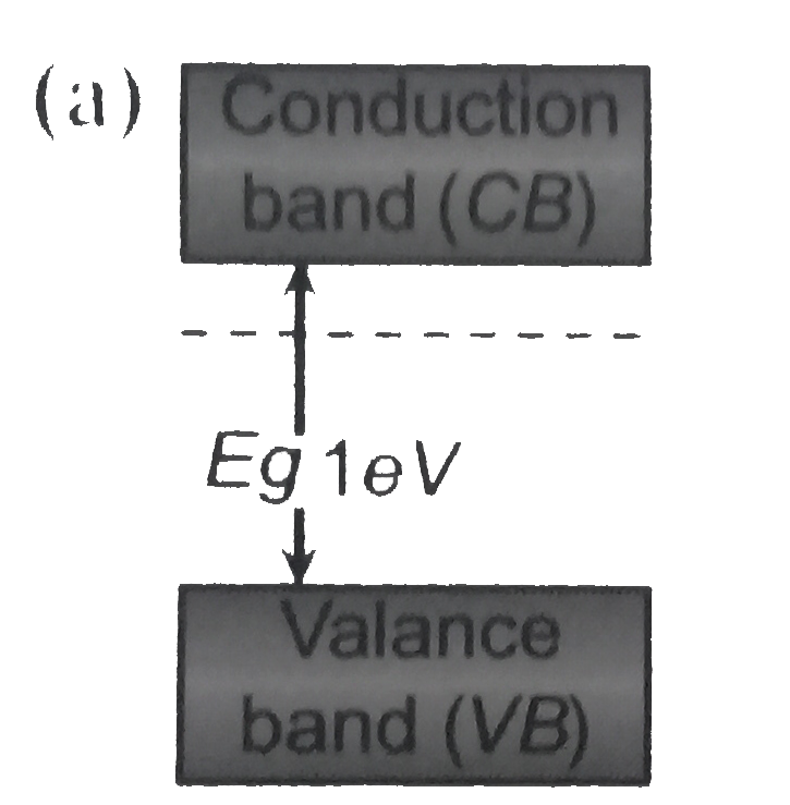 B
B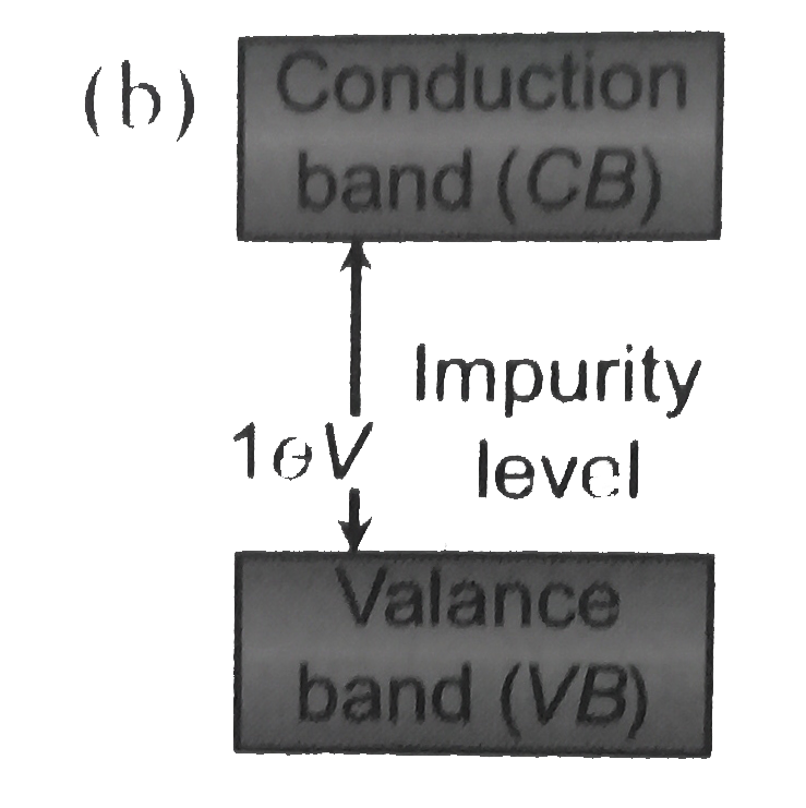 C
C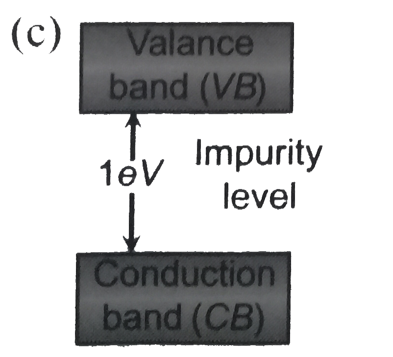 D
D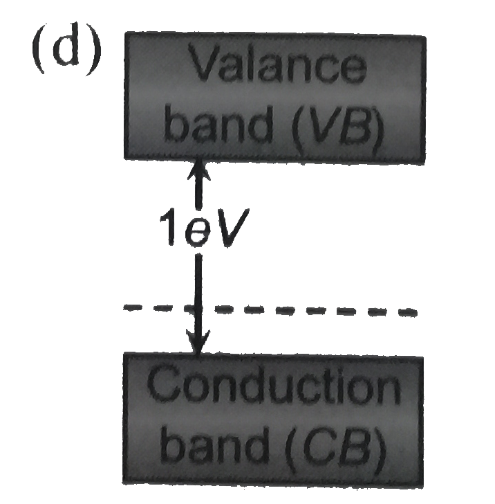
The band structure in n - type semiconductor is
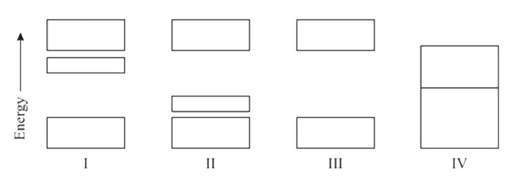 AIBIICIIIDIV
Draw energy band diagram for a n-type extrinsic semiconductor.
View SolutionHow is p-type semiconductor formed? Name the major charge carriers in it. Draw the energy band diagram of a p-type semiconductor.
View SolutionHow is an n-type semiconductor formed? Name the major change carriers in it. Draw the energy band diagram of n-type semiconductor.
View SolutionFrom Energy Band Diagram
View SolutionRead the following passage and then answer question (a) - (e) on the basis of your understanding of the following passage and the related studied concepts.
As per Bohr atom model, in an isolated atom the energy of any of its electrons depends on the orbit in which it revolves and it is characterised by a sharp energy level. However, inside a crystalline solid atoms are close to each other and the outer orbits of electrons from neighbouring atoms would come very close or could even overlap. As a result, each electron will have a different energy level. These different energy levels with continuous energy variation form energy bands.
The energy band which includes the energy levels of the valence electrons is called the valence band. All the valence electrons reside in the valence band. The energy band above the valence band is called the conduction band. Normally the conduction band is empty.
If the lowest level in the conduction band happens to be lower than the highest level of the valence band, electrons from the valence band may easily move into the conduction band and the solid behaves as a conductor.
If there is some gap between the conduction band and the valence band, electrons in the valence band remain confined to it and no free electrons are available in the conduction band. It makes the solid an insulator.
If some of the electrons from the valence band may gain external energy to cross the gap between the conduction band and valence band, these electrons will move into the conduction band and simultaneously create vacant energy levels in the valence band. Therefore, there is a possibility of conduction due to electrons in conduction band as well as due to vacancies in the valence band.
What is the difference between energy band diagram of an insulator and a semiconductor?
View SolutionDraw the energy band diagram of a p-type semiconductor. Deduce an expression for the conductivity of a p-type semiconductor.
View Solution
