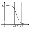
Fig.shows that transfer characteristics of a base biased CE transistor. Which of the following statements are true?
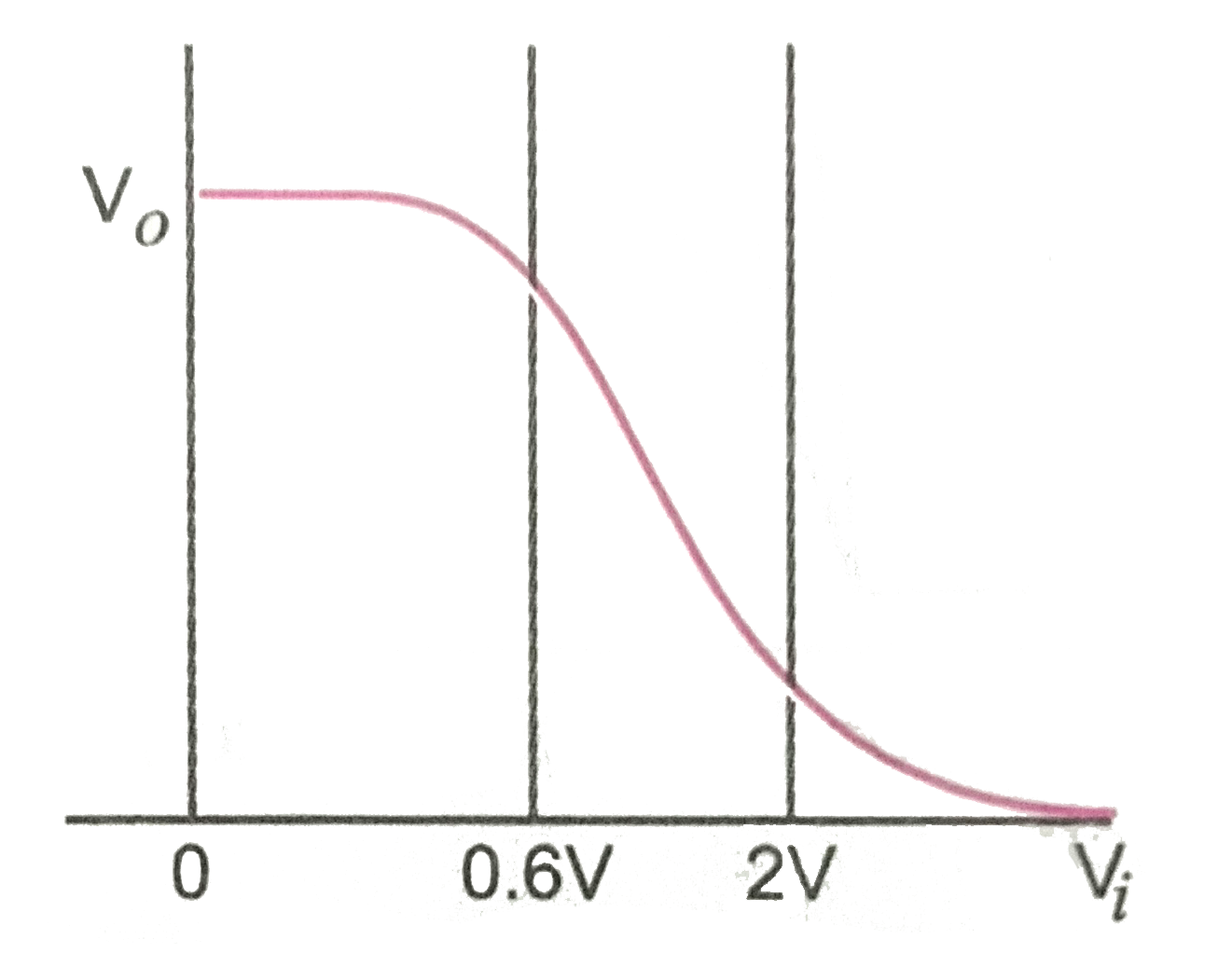
At Vi=1V, it can be used as an amplifier
At Vi=0.5V, it can be used as a switch turned off
At Vi=2.5V, it can be used as a switch turned on
All of these
The correct Answer is:D
From the given transfer characteristics of a base biased common emitter transistor
(i) When Vi=1V, which is in between 0.6 V to 2 V the transistor circuit is in active state and is used as an amplifier.
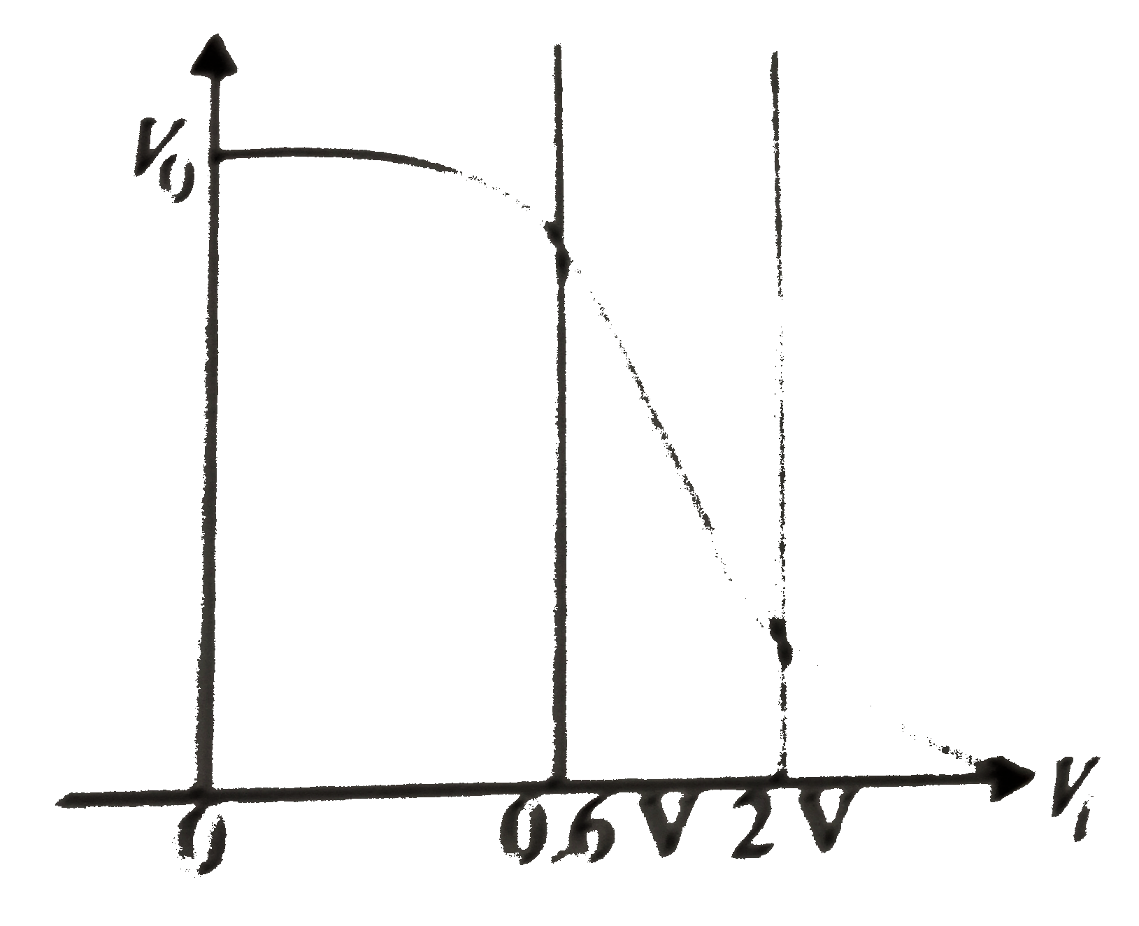
(ii) When Vi=0.5V there is no collector current. The transistor is in cut off state. The transistor circuit can be used as a switch turned off
(iii) When Vi=2.5V, the collector current becomes maximum and transistor is in saturation state and can be used as switch turned on state. So option (a) (b) and (c) are correct
Topper's Solved these Questions
- BOOK - NCERT FINGERTIPSCHAPTER - SEMICONDUCTOR ELECTRONICS : MATERIALS , DEVICES AND SIMPLE CIRCUITS EXERCISE - Digital Electronics And Logic Gates16videos
SEMICONDUCTOR ELECTRONICS : MATERIALS , DEVICES AND SIMPLE CIRCUITS
- BOOK - NCERT FINGERTIPSCHAPTER - SEMICONDUCTOR ELECTRONICS : MATERIALS , DEVICES AND SIMPLE CIRCUITS EXERCISE - Higher Order Thinking Skills8videos
SEMICONDUCTOR ELECTRONICS : MATERIALS , DEVICES AND SIMPLE CIRCUITS
- BOOK - NCERT FINGERTIPSCHAPTER - SEMICONDUCTOR ELECTRONICS : MATERIALS , DEVICES AND SIMPLE CIRCUITS EXERCISE - Special Purpose P-N Junction Diode8videos
SEMICONDUCTOR ELECTRONICS : MATERIALS , DEVICES AND SIMPLE CIRCUITS
- BOOK - NCERT FINGERTIPSCHAPTER - RAY OPTICS AND OPTICAL INSTRUMENTSEXERCISE - Assertion And Reason15videos
RAY OPTICS AND OPTICAL INSTRUMENTS
- BOOK - NCERT FINGERTIPSCHAPTER - WAVE OPTICSEXERCISE - Assertion And Reason15videos
WAVE OPTICS
Similar Questions
Knowledge Check
- Question 1 - Select One
Figure shows the transfer characteristics of a base biased CE transistor. Which of the following statements are true ?
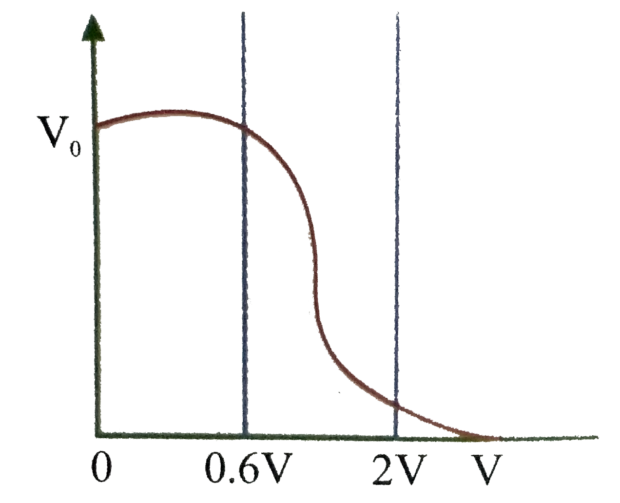
(A) At V1=0.14V transistors is in active state
(B) At V1=1V it can be used as an amplifier
(C) At V1=0.5V, it can be used as a switch turned off
(D) At V1=2.5V, it can be used as switch turned onAA,B,CBB,C,DCA,C,DDA,B,D - Question 2 - Select One
The transfer characteristics of a base biased common in the figure. Which of the following statements are true?
 AAt Vi=1V, it can be used as an amplifier.BAt Vi=0.5V, it can be used as a switch turned off.CAt Vi=2.5V, it can be used as a switch turned on.DAll of these
 - Question 3 - Select One or More
For transistor action, which of the following statements are correct ?
A(a) Base , emitter and collector regions should have similar size and doping concentrationsB(b) The base region must be very thin and lightly dopedC( c) The emitter junction is forward biased and collector junction is reverse biasedD(d) Both the emitter junction as well as the collector junction are forward biased
For transistor action, which of the following statements are correct ?
View SolutionWhich of the following is forward biased?
View SolutionWhich of the following is forward biased?
View SolutionThe transfer characteristics of a base biased transistor has the operation regions, namely, cutoff, active region and saturation region. For using the transistor as an amplifier it has to operate in the
View SolutionThe transfer characteristics of a base biased transistor has the operation regions, namely, cutoff, active region and saturation region. For using the transistor as an amplifier it has to operate in the
View Solution


