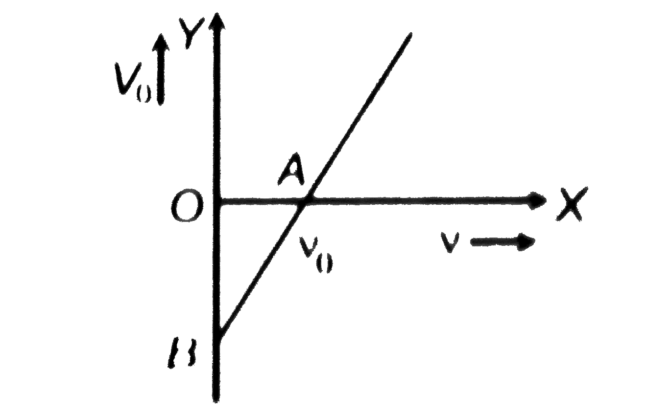
Potential difference across AB i.e., VA−VB is
(##AAK_P5_NEET_PHY_SP5_C18_E04_027_Q01.png" width="80%">)
A
10V
B
8V
C
6 V
D
Zero
Text Solution
The correct Answer is:A
|
Similar Questions
Knowledge Check
The output across the load resistance R is
(##AAK_P7_NEET_PHY_SP7_C29_E04_031_Q01.png" width="80%">AHalf wave rectifiedBFull wave rectifiedCQuarter rectifiedDac(##SASA_NJA_OBJ_BIO_V02_C04_E03_039_Q01.png" width="80%">
A(A)(B)(C)(D)iiiiviiiB(A)(B)(C)(D)iviiiiiiC(A)(B)(C)(D)iviiiiiiD(A)(B)(C)(D)iiiiiiviIn the figure shown
(##AHT_PGT_PHY_C10_E01_006_Q01.png" width="80%">AP>P0BP<P0CP=P0DP=0
In a common emitter transistor circuit, the base current is 40μA , then VBE is
(##AAK_P7_NEET_PHY_SP7_C29_E03_025_Q01.png" width="80%">
View SolutionMatch the following ( ##AAK_MCP_10_NEET_BOT_E10_027_Q01.png" width="80%">
View SolutionThe potential difference between point A and B adjoining figure is<br> (##VMC_NEET_XII_PHY_MOD_04_C13_E05_001_Q01.png" width="80%">
View SolutionThe value of angle r in figure below is
(##AAK_MCP_36_NEET_PHY_E36_017_Q01.png" width="80%">
View SolutionIn an experiment on photoelectric effect the frequency f of the incident light is plotted against the stopping potential V0. The work function of the photoelectric surface si given by ( e is the electronic charge)

View Solution
