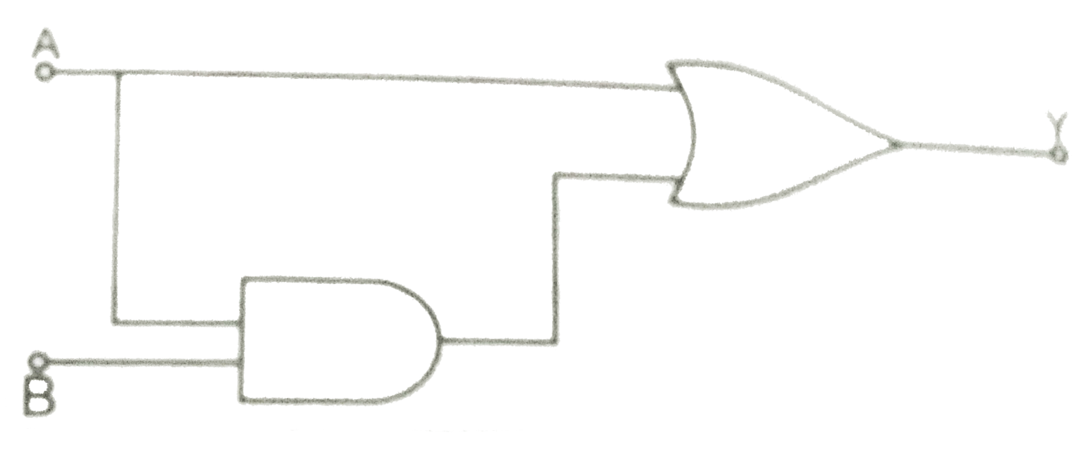
In NOT operation of Y is output and A and B are inputs then truth table in Solution in Kannada
0,0,1,0
1,1,1,0
1,1,0,0
1,1,1,1
The correct Answer is:A
Step by step video, text & image solution for In NOT operation of Y is output and A and B are inputs then truth table in by Physics experts to help you in doubts & scoring excellent marks in Class 12 exams.
Topper's Solved these Questions
- BOOK - MODERN PUBLICATIONCHAPTER - SOLIDS & SEMICONDUCTOR DEVICESEXERCISE - Multiple Choice Questions - LEVEL -I (ASSERTION)5videos
SOLIDS & SEMICONDUCTOR DEVICES
- BOOK - MODERN PUBLICATIONCHAPTER - SOLIDS & SEMICONDUCTOR DEVICESEXERCISE - Multiple Choice Questions - LEVEL -I (PARAGRAPH)6videos
SOLIDS & SEMICONDUCTOR DEVICES
- BOOK - MODERN PUBLICATIONCHAPTER - ROTATIONAL MOTIONEXERCISE - RCQ8videos
ROTATIONAL MOTION
- BOOK - MODERN PUBLICATIONCHAPTER - TRANSFERENCE OF HEAT EXERCISE - Recent Competitive Questions4videos
TRANSFERENCE OF HEAT
Similar Questions
Statement I : In N - type semiconductor , the free electron concentration approximately equals the density of donor atoms .
Statement II : In a forward biased P - N - region is proportional to the change Q of the injected minority carrier holes.01:58View SolutionIn a triode value for a grid voltage Vg=−1.2V , the phase current Ip and plate voltage Vp are given Ip=(−5+0.1V0),Ip in mAandVp in volt . When grid voltage is changed to - 3.2 V at constant plate voltage of 150 V , a plate current of 5 mA is observed , then
Plate resistance Rp is05:01View SolutionThe moment of inertia of a circular disc of radius 2 m and mass 1 kg about an axis passing through the centre of mass but perpendicular to the plane of the disc is 2 kg m2. Its moment of inertia about an axis parallel to this axis but passing through the edge of the disc is :
 02:37View Solution
Two slabs are of the thicknesses d1 and d2. Their thermal conductivities are K1 and K2 respectively They are in series. The free ends of the combination of these two slabs are kept at temperatures θ1 and θ2. Assume θ1>θ2. The temperature θ of their common junction is
02:42View SolutionIn the following circuit, the output Y for all possible inputs A and B is expressed by the truth table:
 01:15View Solution
Express by a truth table, the output Y for all possible input A and B in the following circuit Fig.
 03:27View Solution
The output of a 2-inputs NOR gate is fed as input to a NOT gate. Write down the truth table for the final output of the combination.
View SolutionThe following Fig. shows the input waveforms (A,B) and the output waveform (y) of a gate. Identify the gate and write its truth table.
04:27View SolutionGiven the followig truth table, where A,B are inputs and Y the output
02:57View SolutionIf the Output of two NAND gates is given to input of a NAND gate. Then the truth table will be of
02:33View SolutionFor a given truth table A, B and C are input and Y is the output , then the funtional form of the circuit is
01:25View Solutionदो निवेशी वाले NAND गेट के निर्गत Y को NOT गेट के निवेशी से जोड़ दिया जाता है | संयोजन के अंतिम निर्गत Y के लिए सत्यता सारणी लिखिए|
03:34View SolutionGiven the following truth table where A , B are inputs and Y the output :
ABY001101011110
The output Y is :View SolutionThe truth table given below is for (A and B are the inputs, Y is the output)
02:45View SolutionIn AND operation if Y is output and A and B are inputs the truth table is :
03:59View Solution

