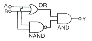
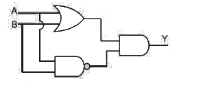
The following configuration of gate is equivalent to :
 Solution in Kannada
NAND
XOR
OR
NOR
The correct Answer is:B
Output of OR gate = A + B
Output of NAND gate = ¯¯¯¯¯¯¯¯A.B
∴ Output Y from AND gate =(A+B).¯¯¯¯¯¯¯¯A.B
=(A+B).(¯¯¯A+¯¯¯B)
=A¯¯¯A+B¯¯¯B+A¯¯¯B+B¯¯¯A
=0+0+A¯¯¯B+B¯¯¯A
=A¯¯¯B+B¯¯¯A
This is expression of XOR gate.
Topper's Solved these Questions
- BOOK - MODERN PUBLICATIONCHAPTER - SOLIDS & SEMICONDUCTOR DEVICESEXERCISE - Multiple Choice Questions - LEVEL -III (Questions From AIEEE/JEE Examination)9videos
SOLIDS & SEMICONDUCTOR DEVICES
- BOOK - MODERN PUBLICATIONCHAPTER - SOLIDS & SEMICONDUCTOR DEVICESEXERCISE - Recent Competitive Questions26videos
SOLIDS & SEMICONDUCTOR DEVICES
- BOOK - MODERN PUBLICATIONCHAPTER - SOLIDS & SEMICONDUCTOR DEVICESEXERCISE - Multiple Choice Questions - LEVEL -I (PARAGRAPH)6videos
SOLIDS & SEMICONDUCTOR DEVICES
- BOOK - MODERN PUBLICATIONCHAPTER - ROTATIONAL MOTIONEXERCISE - RCQ8videos
ROTATIONAL MOTION
- BOOK - MODERN PUBLICATIONCHAPTER - TRANSFERENCE OF HEAT EXERCISE - Recent Competitive Questions4videos
TRANSFERENCE OF HEAT
Similar Questions
Statement - 1 : Sky wave signals are used for long distance radio communication. These signals are in general, less stable than ground wave signals. Statement - 2 : The state of ionosphere varies from hour to hour, day to day and season to season.
02:42View SolutionThe forbidden energy gap in Ge in 0.72 eV Given, hc=12400 eV−Å The maximum wavelength of radiation that will generate electron hole pair is
01:44View SolutionIn a triode value for a grid voltage Vg=−1.2V , the phase current Ip and plate voltage Vp are given Ip=(−5+0.1V0),Ip in mAandVp in volt . When grid voltage is changed to - 3.2 V at constant plate voltage of 150 V , a plate current of 5 mA is observed , then
Plate resistance Rp is02:15View SolutionThe moment of inertia of a circular disc of radius 2 m and mass 1 kg about an axis passing through the centre of mass but perpendicular to the plane of the disc is 2 kg m2. Its moment of inertia about an axis parallel to this axis but passing through the edge of the disc is :
 04:04View Solution
Two slabs are of the thicknesses d1 and d2. Their thermal conductivities are K1 and K2 respectively They are in series. The free ends of the combination of these two slabs are kept at temperatures θ1 and θ2. Assume θ1>θ2. The temperature θ of their common junction is
02:47View SolutionThe figure shows two NAND gates followed by a NOR gate. The system is equivalent to the following logic gate
04:02View SolutionThe NOR gate is logically equivalent to an OR gate followed by :-
01:33View SolutionThe following congiguration of gates is equivalent to
02:12View SolutionThe figure shows NAND gates followed by a NOR gate . The system is equivalent to the following logic gate .
01:55View Solutionनिम्नलिखित द्वारों का अभिविन्यास तुल्य है :
 01:36View Solution
The following configuration of gate is equivalent to which gate? Write its truth table.
01:50View SolutionTwo inputs of NAND gates are shorted, what is the equivalent logic gate for this configuration?
01:50View SolutionThe following network of gates is equivalent to
03:32View SolutionTwo inputs of NAND gate are shortened. This gate is equivalent to
01:07View SolutionThe following gate is equivalent to
 01:40View Solution
Two inputs of NAND gate are shortened. This gate is equivalent to
02:41View Solution

