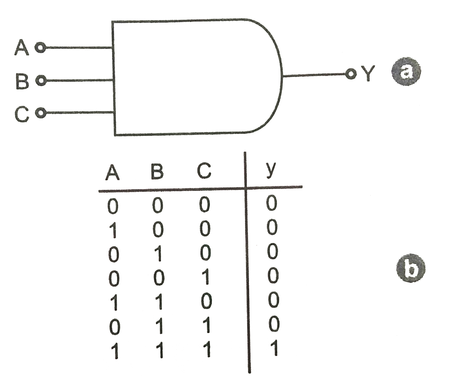
Draw the logic symbol of NAND gate and give its Truth table
Step-by-Step Solution:
Step 1: Draw the Logic Symbol of NAND Gate
The logic symbol of a NAND gate can be constructed by taking the symbol of an AND gate and adding a small circle (representing NOT) at the output.
- AND Gate Symbol: The AND gate has two inputs (A and B) and one output (Y). The shape is typically a flat-ended shape with two inputs on the left and one output on the right.
- Adding NOT: To convert the AND gate into a NAND gate, place a small circle (representing negation) at the output of the AND gate.
The final NAND gate symbol looks like this:
A−−−−∣||AND⊢−o−−−YB−−−−||
Step 2: Create the Truth Table for NAND Gate
The truth table for a NAND gate shows the output for all possible combinations of its inputs A and B. The NAND gate outputs a low signal (0) only when both inputs are high (1).
Here’s how to construct the truth table:
| A | B | A AND B (X) | NAND Output (Y) |
|---|---|-------------|------------------|
| 0 | 0 | 0 | 1 |
| 0 | 1 | 0 | 1 |
| 1 | 0 | 0 | 1 |
| 1 | 1 | 1 | 0 |
- Explanation:
- When both A and B are 0, the output of the AND gate (X) is 0, and the NAND output (Y) is 1 (since NOT of 0 is 1).
- When A is 0 and B is 1, X is still 0, and Y is 1.
- When A is 1 and B is 0, X is 0, and Y is 1.
- When both A and B are 1, X is 1, and Y is 0 (since NOT of 1 is 0).
Final Answer:
1. Logic Symbol of NAND Gate:
A−−−−∣||AND⊢−o−−−YB−−−−||
2. Truth Table for NAND Gate:
| A | B | NAND Output (Y) |
|---|---|------------------|
| 0 | 0 | 1 |
| 0 | 1 | 1 |
| 1 | 0 | 1 |
| 1 | 1 | 0 |
- Adding NOT: To convert the AND gate into a NAND gate, place a small circle (representing negation) at the output of the AND gate.
|---|---|-------------|------------------|
| 0 | 0 | 0 | 1 |
| 0 | 1 | 0 | 1 |
| 1 | 0 | 0 | 1 |
| 1 | 1 | 1 | 0 |
- When both A and B are 0, the output of the AND gate (X) is 0, and the NAND output (Y) is 1 (since NOT of 0 is 1).
- When A is 0 and B is 1, X is still 0, and Y is 1.
- When A is 1 and B is 0, X is 0, and Y is 1.
- When both A and B are 1, X is 1, and Y is 0 (since NOT of 1 is 0).
A−−−−∣||AND⊢−o−−−YB−−−−||
|---|---|------------------|
| 0 | 0 | 1 |
| 0 | 1 | 1 |
| 1 | 0 | 1 |
| 1 | 1 | 0 |
Topper's Solved these Questions
- SEMICONDUCTOR ELECTRONICS METERIALS DEVICES AND SIMPLE CIRCUITS BOOK - MODERN PUBLICATIONCHAPTER - SEMICONDUCTOR ELECTRONICS METERIALS DEVICES AND SIMPLE CIRCUITS EXERCISE - REVISION EXERCISES (ADDITOINAL QUESTION)
9 Videos
- SEMICONDUCTOR ELECTRONICS METERIALS DEVICES AND SIMPLE CIRCUITS BOOK - MODERN PUBLICATIONCHAPTER - SEMICONDUCTOR ELECTRONICS METERIALS DEVICES AND SIMPLE CIRCUITS EXERCISE - REVISION EXERCISES(FILL IN THE BLANKS )
10 Videos
- SEMICONDUCTOR ELECTRONICS METERIALS DEVICES AND SIMPLE CIRCUITS BOOK - MODERN PUBLICATIONCHAPTER - SEMICONDUCTOR ELECTRONICS METERIALS DEVICES AND SIMPLE CIRCUITS EXERCISE - HIGER ORDER THINKING SKILLS & ADVANCED LEVEL
11 Videos
- RAY OPTICS AND OPTICAL INSTRUMENTSBOOK - MODERN PUBLICATIONCHAPTER - RAY OPTICS AND OPTICAL INSTRUMENTSEXERCISE - CHAPTER PRACTICE TEST
14 Videos
- WAVE OPTICALBOOK - MODERN PUBLICATIONCHAPTER - WAVE OPTICALEXERCISE - CHAPTER PRACTICE TEST
7 Videos
Similar Questions
Give the logic symbol of NAND gate.
View SolutionGive the logic symbol of AND gate.
View SolutionGive the logic symbol of NOR gate.
View SolutionDraw the logic symbol of the gate given below:

View SolutionWhat is AND gate ? Draw its truth table.
View Solution(a) Draw a neat diagram for a full wave rectifier circuit
(b) Draw the logic gate symbol and the truth table for a NAND gate with tow inputs
(c ) In an n-p-n tranasistor circuit the collector current is 10 mA if 95% of the enemitter current reach the collector what is the base current
View Solution
Name of gate obtained from the combination of gates shown in the figure. Draw its logic symbol. Write the truth table of the combination.
View SolutionThe output of and AND gate is connected to both the inputsof a NAND gate. Draw the logic circuit of this combinationn of gates and write its truth table.
View SolutionWhat is a logic gate? Draw the symbol and give the truth table for NOT gate. Why NOT gate is called inverter?
View SolutionFind the output y of the logic gate whose symbol Is shown in Fig. and give a truth table for the same.

View Solution
