Draw a diagram of an illuninated p-n junction solar cell
Step-by-Step Solution to Draw an Illuminated P-N Junction Solar Cell
1. Draw the P-N Junction:
- Start by drawing a horizontal line to represent the junction between the p-type and n-type semiconductor materials.
- Label the left side as "P-Type Material" and the right side as "N-Type Material".
2. Indicate Majority Carriers:
- On the p-type side, draw several circles to represent holes (positive charge carriers). Label them as "Holes (Majority)".
- On the n-type side, draw several dots to represent electrons (negative charge carriers). Label them as "Electrons (Majority)".
3. Show the Charge Distribution:
- Draw a wall of negatively charged ions on the n-type side and a wall of positively charged ions on the p-type side, indicating the built-in electric field.
- Label these walls as "Negatively Charged Ions" on the n-side and "Positively Charged Ions" on the p-side.
4. Illustrate Photon Illumination:
- Draw arrows coming from the top to represent incoming photons (solar radiation). Label these arrows as "Photons (hν)".
5. Indicate Electron-Hole Pair Generation:
- Draw small circles and dots around the junction area to represent the generation of electron-hole pairs due to photon absorption. Label this area as "Electron-Hole Pair Generation".
6. Show Movement of Carriers:
- Draw arrows indicating the movement of electrons from the p-side to the n-side and holes from the n-side to the p-side due to the electric field. Label these arrows as "Electron Movement" and "Hole Movement".
7. Label the Photovoltaic Effect:
- Indicate that the p-side becomes positively charged and the n-side becomes negatively charged, resulting in a photovoltage. Label this as "Photovoltage Generation".
8. Connect External Circuit:
- Draw a simple circuit with a resistor connected between the p-side and n-side to indicate the flow of current. Label the direction of current flow from the positive terminal (p-side) to the negative terminal (n-side).
9. Final Touches:
- Add any additional labels or notes that clarify the operation of the solar cell, such as "Current Flow" and "External Load".
- Start by drawing a horizontal line to represent the junction between the p-type and n-type semiconductor materials.
- Label the left side as "P-Type Material" and the right side as "N-Type Material".
- On the p-type side, draw several circles to represent holes (positive charge carriers). Label them as "Holes (Majority)".
- On the n-type side, draw several dots to represent electrons (negative charge carriers). Label them as "Electrons (Majority)".
- Draw a wall of negatively charged ions on the n-type side and a wall of positively charged ions on the p-type side, indicating the built-in electric field.
- Label these walls as "Negatively Charged Ions" on the n-side and "Positively Charged Ions" on the p-side.
- Draw arrows coming from the top to represent incoming photons (solar radiation). Label these arrows as "Photons (hν)".
- Draw small circles and dots around the junction area to represent the generation of electron-hole pairs due to photon absorption. Label this area as "Electron-Hole Pair Generation".
- Draw arrows indicating the movement of electrons from the p-side to the n-side and holes from the n-side to the p-side due to the electric field. Label these arrows as "Electron Movement" and "Hole Movement".
- Indicate that the p-side becomes positively charged and the n-side becomes negatively charged, resulting in a photovoltage. Label this as "Photovoltage Generation".
- Draw a simple circuit with a resistor connected between the p-side and n-side to indicate the flow of current. Label the direction of current flow from the positive terminal (p-side) to the negative terminal (n-side).
- Add any additional labels or notes that clarify the operation of the solar cell, such as "Current Flow" and "External Load".
Topper's Solved these Questions
- SEMICONDUCTOR ELECTRONICS METERIALS DEVICES AND SIMPLE CIRCUITS BOOK - MODERN PUBLICATIONCHAPTER - SEMICONDUCTOR ELECTRONICS METERIALS DEVICES AND SIMPLE CIRCUITS EXERCISE - REVISION EXERCISES( LONG ANSWER QUESTIONS)
11 Videos
- SEMICONDUCTOR ELECTRONICS METERIALS DEVICES AND SIMPLE CIRCUITS BOOK - MODERN PUBLICATIONCHAPTER - SEMICONDUCTOR ELECTRONICS METERIALS DEVICES AND SIMPLE CIRCUITS EXERCISE - REVISION EXERCISES (NUMERICAL PROBLEMS )
15 Videos
- SEMICONDUCTOR ELECTRONICS METERIALS DEVICES AND SIMPLE CIRCUITS BOOK - MODERN PUBLICATIONCHAPTER - SEMICONDUCTOR ELECTRONICS METERIALS DEVICES AND SIMPLE CIRCUITS EXERCISE - REVISION EXERCISES(FILL IN THE BLANKS )
10 Videos
- RAY OPTICS AND OPTICAL INSTRUMENTSBOOK - MODERN PUBLICATIONCHAPTER - RAY OPTICS AND OPTICAL INSTRUMENTSEXERCISE - CHAPTER PRACTICE TEST
14 Videos
- WAVE OPTICALBOOK - MODERN PUBLICATIONCHAPTER - WAVE OPTICALEXERCISE - CHAPTER PRACTICE TEST
7 Videos
Similar Questions
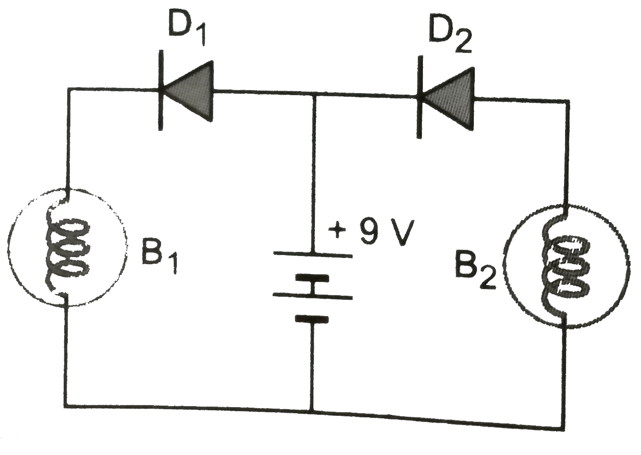
In the following diagram, which bulb out of B1 andB2 will glow and why?

Draw a diagram of an illuminated p-n junction solar cell
Explain briefly the three processes due to which generation of emf takes place in a solar cell.
View SolutionDraw a diagram of an illuminated p-n junction solar cell.
View Solution
Knowledge Check
In a p−n junction
AP and N both are at same potentialBHigh potential at N side and low potential at P sideCHigh potential P side and low potential at N sideDLow potential at N side and zero potential at P sideIn a p-n junction ,
Anew holes and conduction electorns are produced continuously throughout the materialBnew holes and conduction electrons are produced continuously throughout the material except in the depletion regionCholes and conduction electrons recombine continously throughout the materialDholes and conduction electrons recombine continuously throughout the material except in the depletion region.In an unbiased p-n junction,
Apotential at p is more than that at nBpotential at p is less than that at nCpotential at p is equal to that at nDpotential at p is positive and that at n is negative
