How is junction diode formed ? Discuss the working of a junction diode as a full-wave rectifier.
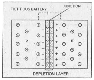
Formation of junction diode. When a p-type crystal is placed in contact with n-type crystal so as to form one piece, the assembly so obtained is called p-n junction or junction diode or crystal diode. The surface of contact of p-type and n-type crystals is called junction. In the psection, holes are the majority carriers while in n-section, the majority carriers are electrons. Due to high concentration of different types of charge carriers in the two sections, holes from p-region diffuse into n-region and electrons from n-region diffuse into p-region. In both cases, when an electron meets a hole they cancel the effect of each other and as a result, a thin layer at the junction becomes devoid of charge carriers. This is called depletion

layer as shown in the figure. The thickness of depletion layer is of the order of 10−6 m.
Due to the migration of holes and electrons, the two sections of the junction diode no longer remain neutral. The p-section of the junction diode becomes slightly negative, while the n-section is rendered positive. Due to this, there is a potential gradient in the depletion layer, negative on the p-side and positive on the n-side. In other

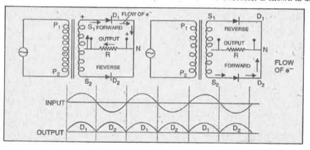
Working. During the positive half of input AC,D1 is forward biased and D2 reverse biased. Hence the current flows through the upper circuit as shown. During negative half, lower portion (D2) is forward biased and upper (D1) is reverse biased.
words, it appears as if some fictitious battery is connected across the junction with its negative pole connected topregion and positive pole connected to n-region. The potential difference developed across the junction diode due to migration of majority carriers is called potential barrier.
Full wave rectifier. The circuit diagram using junction diode as full wave rectifier is shown in the figure.
Thus during each half, we get the current either from D1 and from D2. The output voltage is unidirectional.
Topper's Solved these Questions
- BOOK - MBD -HARYANA BOARDCHAPTER - MODEL TEST PAPER (SOLVED)EXERCISE - SHORT ANSWER TYPE QUESTIONS7videos
MODEL TEST PAPER (SOLVED)
- BOOK - MBD -HARYANA BOARDCHAPTER - MAGNETISMEXERCISE - OBJECTIVE TYPE QUESTIONS17videos
MAGNETISM
- BOOK - MBD -HARYANA BOARDCHAPTER - MODEL TEST PAPER - 2EXERCISE - SET - D ( LONG ANSWER TYPE QUESTIONS)4videos
MODEL TEST PAPER - 2
Similar Questions
What is rectifier explain the working of junction diode as a full wave rectifier diagram
View SolutionWhat is a p-n junction diode? Define the term 'dynamic resistance' for the junction diode. With the help of a circuit diagram explain the working of a p-n junction diode as a full wave rectifier.
View SolutionWhat is rectifier explain the working of junction diode as a full wave rectifier diagram
View SolutionExplain with the help of a circuit diagram, the working of a p-n junction diode as a half-wave rectifier.
View SolutionExplain with the help of a circuit diagram, the working of a p−n junction diode as a half wave rectifier.
View SolutionExplain with the help of a circuit diagram, the working of a p−n junction diode as a half wave rectifier.
View SolutionWith the help of circuit diagram explain, the working of p-n junction diode as half wave rectifier.
View SolutionExplain with a neat diagram, how a p-n junction diode is used as a half wave rectifier.
View SolutionWhat is a rectifier ? How a p-n junction diode can be used as a rectifier?
View SolutionHow is zener diode fabricated so as to make it a special purpose diode the significance of brekdown votlage explain brielfy with the help of a cirucit diagram how a p-n junction diode works as a half wave rectifier
View Solution
