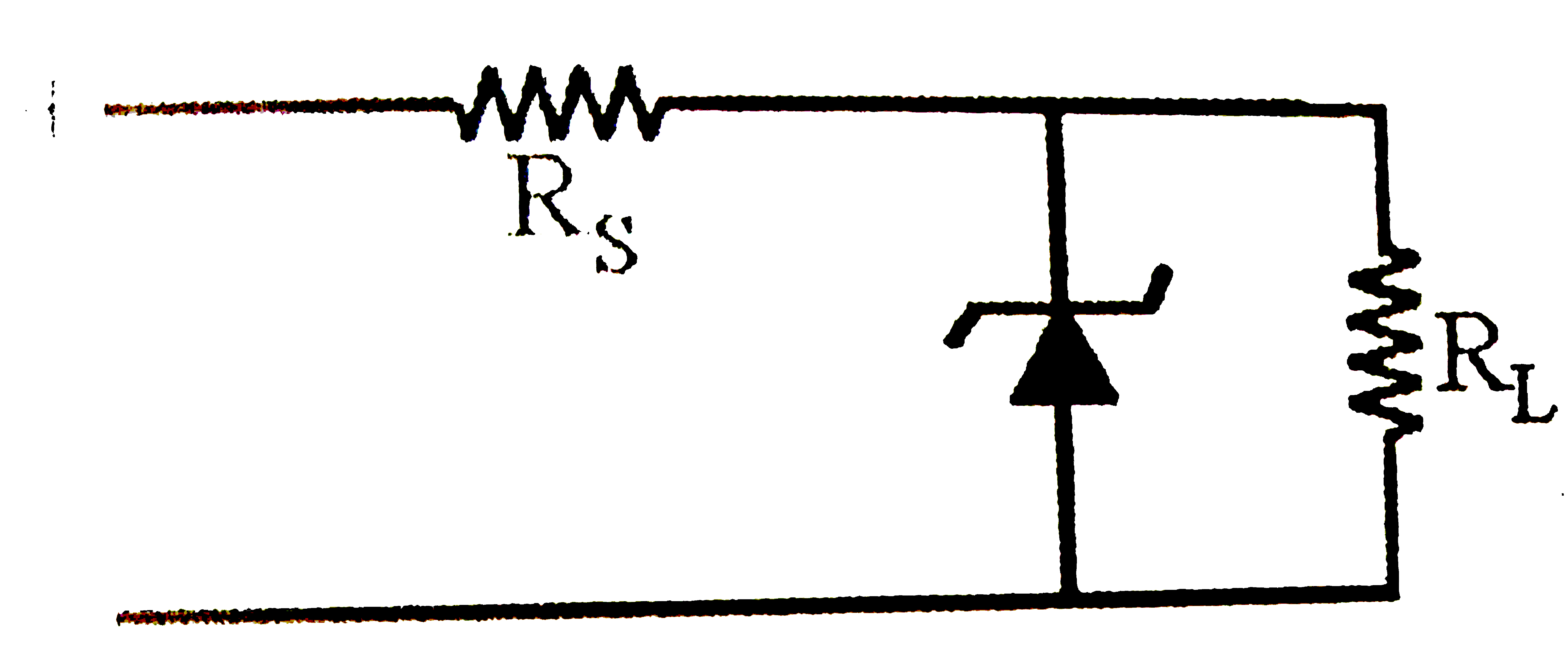
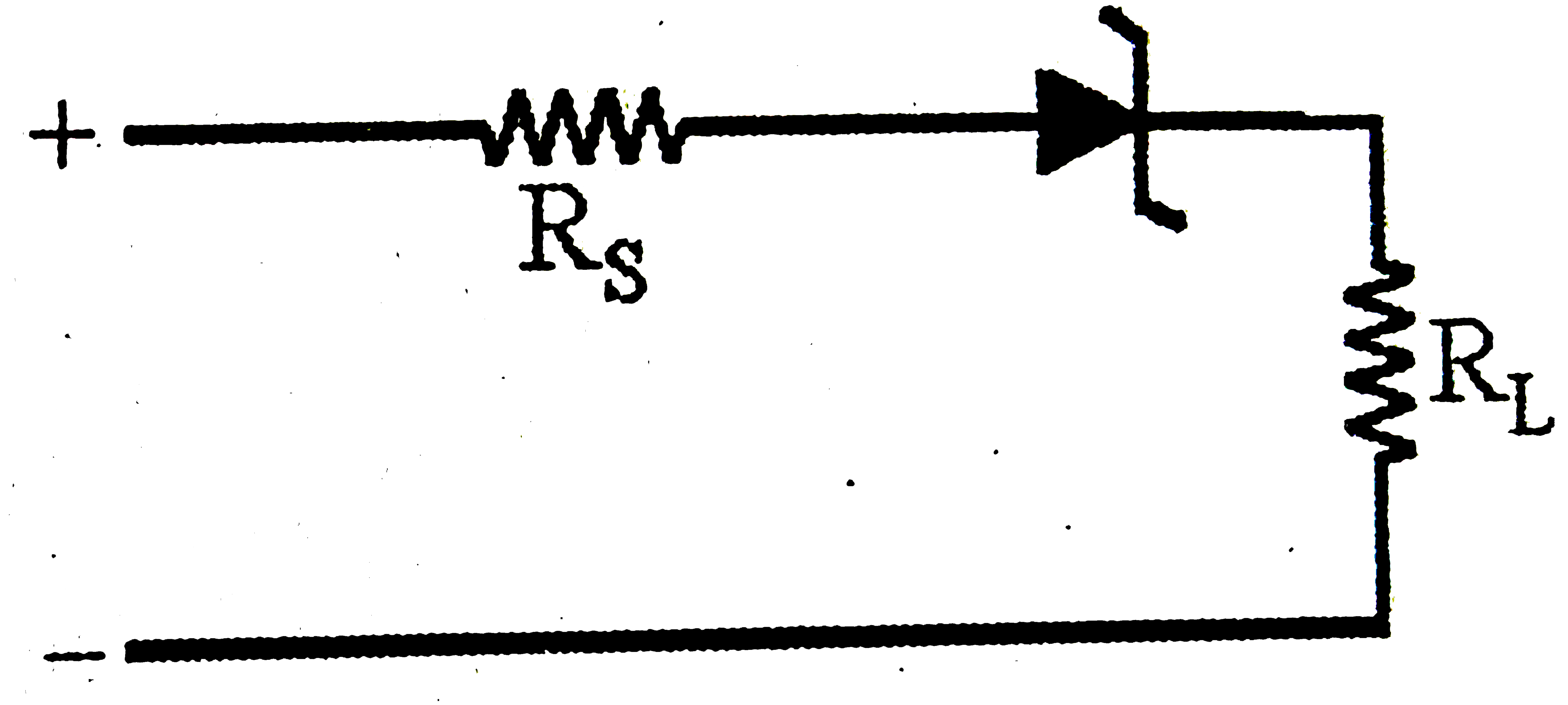
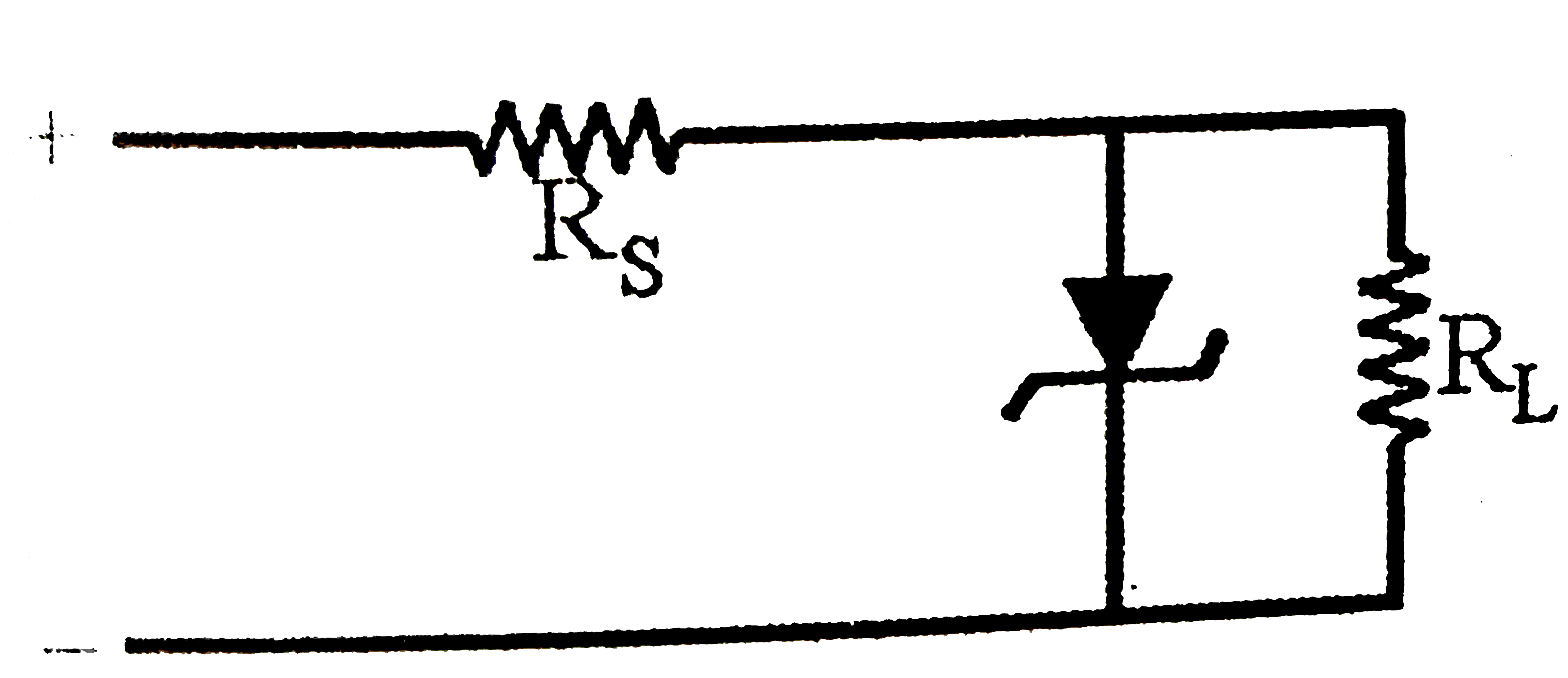
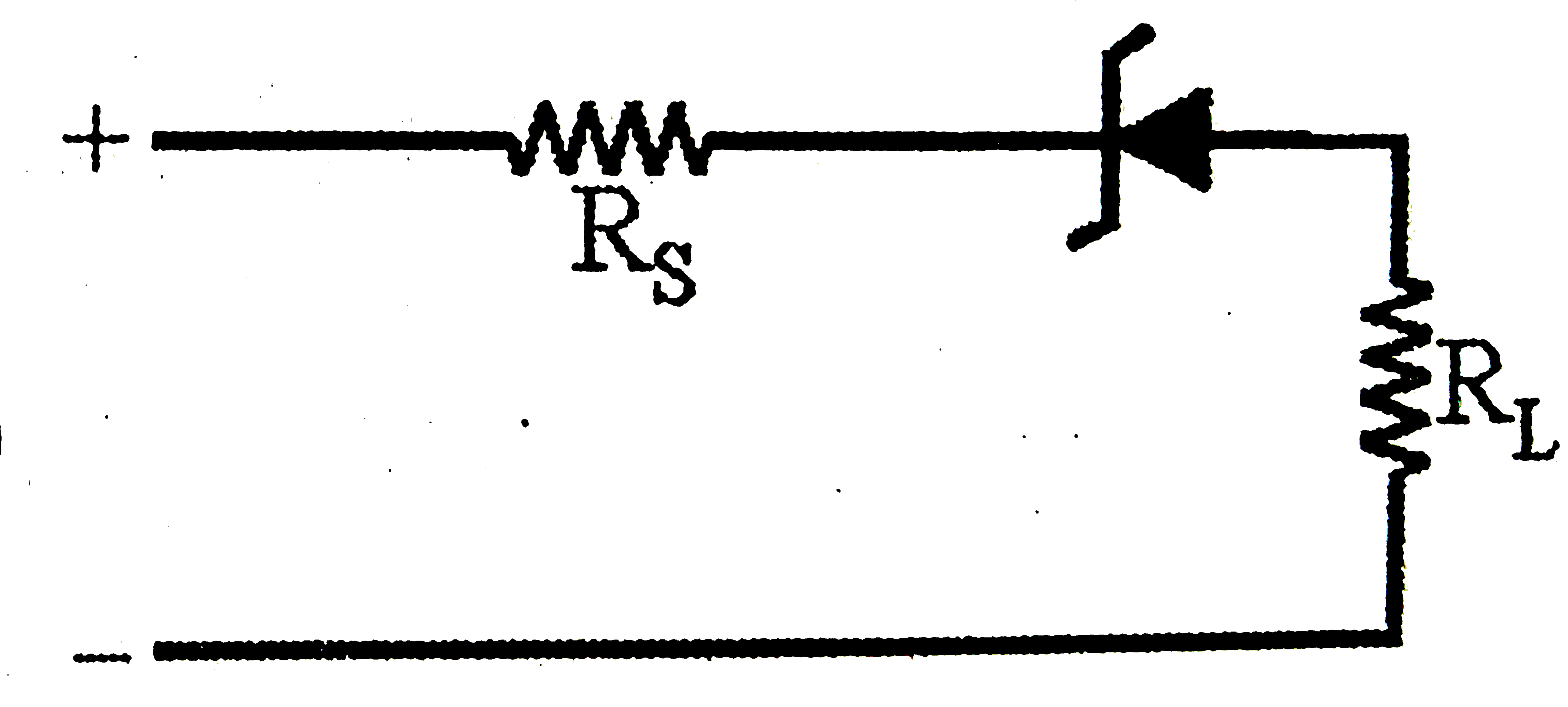
A zener diode is fabricated by heavily doping both p- and -sides of the junction. Explain why ? Breifly explain the use of zener diode as a d.c. voltage regulator with the help of a circuit diagram.
Text Solution
Zener diode is icated by heavily doping both p- andn- sides of the p-n junction. As a result, the depletion region formed is very thin, even less than 106 m, and consequently the electric field at the junction is extremely high (of the order of 5×10⁶ V/m or even more) even for a small reverse bias voltage of about 5 V and breakdown voltage has a low value of about 5 V.
A zener diode is used to get a constant d.c. voltage from the unregulated filtered output of a full-wave rectifier. The circuit diagram is shown in . The unregulated d.c. voltage is connected to zener diode through a series resistance Rs, . Of course zener diode is connected in reverse bias arrangement. Output voltage is obtained across load resistor RL which is joined in parallel to zener diode .
If the zener voltage increases, the current through Rs and zener diode also increases. This increase the voltage drop across Rs but voltage drop across zener diode (or load RI) remains constant. This is because in the breakdown region, zener voltage remains constant even though the current through the zener diode changes. Again if the input d.c. voltage decreases, current through Rs and zener diode decreases. The voltage drop across Rs decreases but voltage drop across zener diode (or load RI) remains practically constant. Thus, any increase/decrease in the input voltage Vi results in an increase/decrease of the voltage drop across Rs without any change in voltage across the zener diode. Hence, the zener diode acts as a voltage regulator, in which the output d.c. voltage is constant at the zener (breakdown) voltage Vz of the zener diode.

|
Topper's Solved these Questions
- SEMICONDUCTOR ELECTRONICS : MATERIALS, DEVICES AND SIMPLE CIRCUITSBOOK - U-LIKE SERIESCHAPTER - SEMICONDUCTOR ELECTRONICS : MATERIALS, DEVICES AND SIMPLE CIRCUITSEXERCISE - SELF ASSESSMENT TEST (MULTIPE CHOICE QUESTIONS )SECTION A
3 Videos
- SEMICONDUCTOR ELECTRONICS : MATERIALS, DEVICES AND SIMPLE CIRCUITSBOOK - U-LIKE SERIESCHAPTER - SEMICONDUCTOR ELECTRONICS : MATERIALS, DEVICES AND SIMPLE CIRCUITSEXERCISE - SECTION B
1 Videos
- SEMICONDUCTOR ELECTRONICS : MATERIALS, DEVICES AND SIMPLE CIRCUITSBOOK - U-LIKE SERIESCHAPTER - SEMICONDUCTOR ELECTRONICS : MATERIALS, DEVICES AND SIMPLE CIRCUITSEXERCISE - SHORT ANSWER QUESTIONS
28 Videos
- RAY OPTICS AND OPTICAL INSTRUMENTSBOOK - U-LIKE SERIESCHAPTER - RAY OPTICS AND OPTICAL INSTRUMENTSEXERCISE - SELF ASSESSMENT TEST (SECTION B)
3 Videos
- WAVE OPTICSBOOK - U-LIKE SERIESCHAPTER - WAVE OPTICSEXERCISE - SELF ASSESSMENT TEST SECTION C (VERY SHORT ANSWER QUESTIONS)
4 Videos
Similar Questions
Knowledge Check
Zener diode has both p and n-ends heavily doped so that-
Ait has small thickness of depletion regionBit has large thickness of depletion region due to large recombinationCit has large reverse bias voltageDit has weak reverse current when reverse biasedA zener diode is to be used as a voltage regulator. Identify the correct set up.
A B
B C
C D
D
Zener diode is fabricated by heavily doping both p- and n-sides of the junction so breakdown occurs at a voltage of about 5 V in reverse bias.
View SolutionZener Diode As Voltage Regulator
View SolutionWhat is Zener diode? How is it used as voltage regulator?
View SolutionZener Breakdown | Zener diode and zener diode as voltage regulator
View SolutionDraw a lablled circuit diagram of a Zener diode as a voltage regulator.
View SolutionA zener diode is to be used as a voltage regulator. Identify the correct set up.
View Solution
