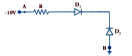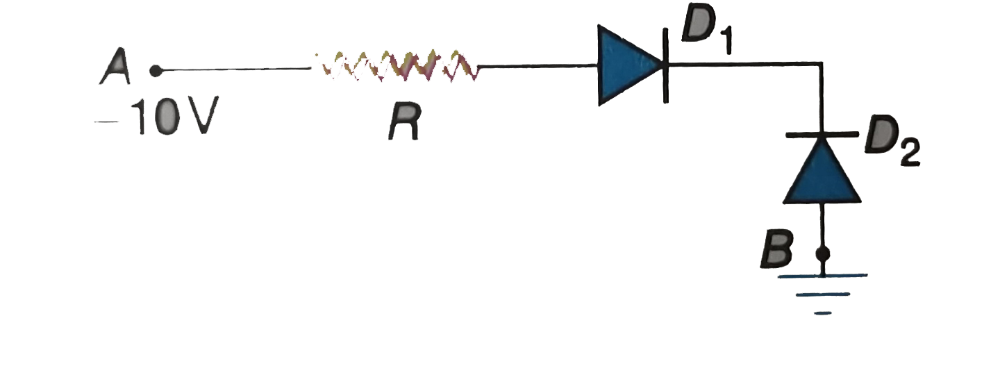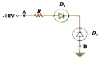
In figure, assuming the diodes to be ideal, Solution in Gujrati
D1 is forward biased and D2 is reverse biased and hence current flows from A to B
D2 is forward biased and D1 is reverse biased and hence no current flows from B to A and vice versa.
D1 and D2 are both forward biased and hence current flows from A to B.
D1andD2 are both reverse biased and hence no current flows from A to B and vice versa.
The correct Answer is:B
D2 is forward biased and D1 is reverse biased and hence no current flows from B to A and vice versa.
For diode D1,VA=−10VandVK=0⇒VA<VR⇒D1 is reverse biased. Hence its resistance would be R1=∞(∵D1 is an ideal diode)
For diode D2,VA=0andVK=−10V⇒VA>VK⇒D2 is forward biased. Hence its resistance would be R2=0.(∵D2 is an ideal diode)
Here, D1andD2 are connected in series and so its equivalent resistance R=R1+R2=∞+0=∞ and so current will not flow, neither from A to B nor from B to A.
⇒ Option (B) is correct.
Topper's Solved these Questions
- BOOK - KUMAR PRAKASHANCHAPTER - SEMICONDUCTOR ELECTRONICS : MATERIALS, DEVICES AND SIMPLE CIRCUITS EXERCISE - Section-C: NCERT Exemplar Solution (Multiple Choice Qustion (More than One Options))8videos
SEMICONDUCTOR ELECTRONICS : MATERIALS, DEVICES AND SIMPLE CIRCUITS
- BOOK - KUMAR PRAKASHANCHAPTER - SEMICONDUCTOR ELECTRONICS : MATERIALS, DEVICES AND SIMPLE CIRCUITS EXERCISE - Section-C: NCERT Exemplar Solution (Very Short Answer Type Questions)6videos
SEMICONDUCTOR ELECTRONICS : MATERIALS, DEVICES AND SIMPLE CIRCUITS
- BOOK - KUMAR PRAKASHANCHAPTER - SEMICONDUCTOR ELECTRONICS : MATERIALS, DEVICES AND SIMPLE CIRCUITS EXERCISE - Section-B : Numericals (Numerical From .DARPAN. Based On Textbook)14videos
SEMICONDUCTOR ELECTRONICS : MATERIALS, DEVICES AND SIMPLE CIRCUITS
- BOOK - KUMAR PRAKASHANCHAPTER - SAMPLE QUESTION PAPER EXERCISE - PART-B SECTION-C5videos
SAMPLE QUESTION PAPER
- BOOK - KUMAR PRAKASHANCHAPTER - WAVE OPTICSEXERCISE - SECTION-D (MULTIPLCE CHOICE QUESTIONS (MCQS)) (MCQS FROM DARPAN BASED ON TEXTBOOK)239videos
WAVE OPTICS
Similar Questions
When an electric field is applied across a semiconductor
02:08View SolutionWhy are elemental dopants for Silicon on Germanium usually chosen from group XIII on group XV ?
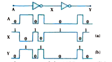
02:02View SolutionA logic circuit is shown in the diagram. Draw the output signal at the point X and Y for the input signal shown in the figure at point A.
 01:43View Solution
Two charges –q and +q are located at points (0, 0, –a) and (0, 0, a), respectively.
(a) What is the electrostatic potential at the points (0, 0, z) and (x, y, 0) ?
(b) Obtain the dependence of potential on the distance r of a point from the origin when r/a>>1 .
(c) How much work is done in moving a small test charge from the point (5,0,0) to (–7,0,0) along the x-axis? Does the answer change if the path of the test charge between the same points is not along the x-axis?01:35View SolutionAccording to particle theory of light what is the velocity of light in a dense medium, compared to that in rare medium ?
03:19View SolutionIn figure , assuming the diodes to be ideal ,
01:25View SolutionAssuming that the junction diode is ideal the current through the diode is :-
02:34View SolutionAssuming that the junction diode is ideal, the current in arrangement shown in figure is
04:49View SolutionIn a figure given alongside assuming the diodes to be ideal
 View Solution
Assuming that the function diode is ideal, the current in the arrangement shown in figure is .
01:33View SolutionAssuming that the junction diode is ideal, the current in arrangement shown in figure is
 01:55View Solution
Four silicon diodes are connected as shown in the figure. Assuming the diodes to be ideal. The current through the resistor R is
03:06View SolutionIn Fig 1.50 assuming the diodes to be ideal
 02:02View Solution
In Fig assuming the diodes to be ideal :
 03:15View Solution
Assuming that the junction diode is ideal , in the circuit shown here , the current through the diode is :
02:02View Solution

