In the depletion region of a diode Solution in Gujrati
there are no mobile charges
equal number of holes and electrons exist, making the region neutral.
recombination of holes and electrons has taken place.
immobile charged ions exist.
The correct Answer is:A, B, D
Inside the depletion layer, on one side of junction, there are positive ions and on the other side of it, there are negative ions. These ions are bonded in the crystalline structure and hence can not move. Thus, option (A) is correct.
Inside a depletion layer, as many electrons are freed by breaking of covalent bonds, that many holes are produced. Hence depletion layer is electrically neutral. Hence option (B) is also correct.
Inside a depletion layer, there are positive and negative ions at fixed locations in the crystalline structure. Thus, option (D) is also correct.
Topper's Solved these Questions
- SEMICONDUCTOR ELECTRONICS : MATERIALS, DEVICES AND SIMPLE CIRCUITS BOOK - KUMAR PRAKASHANCHAPTER - SEMICONDUCTOR ELECTRONICS : MATERIALS, DEVICES AND SIMPLE CIRCUITS EXERCISE - Section-C: NCERT Exemplar Solution (Very Short Answer Type Questions)
6 Videos
- SEMICONDUCTOR ELECTRONICS : MATERIALS, DEVICES AND SIMPLE CIRCUITS BOOK - KUMAR PRAKASHANCHAPTER - SEMICONDUCTOR ELECTRONICS : MATERIALS, DEVICES AND SIMPLE CIRCUITS EXERCISE - Section-C: NCERT Exemplar Solution (Short Answer Type Questions)
8 Videos
- SEMICONDUCTOR ELECTRONICS : MATERIALS, DEVICES AND SIMPLE CIRCUITS BOOK - KUMAR PRAKASHANCHAPTER - SEMICONDUCTOR ELECTRONICS : MATERIALS, DEVICES AND SIMPLE CIRCUITS EXERCISE - Section-C: NCERT Exemplar Solution (Multiple Choice Qustion (MCQs) )
8 Videos
- SAMPLE QUESTION PAPER BOOK - KUMAR PRAKASHANCHAPTER - SAMPLE QUESTION PAPER EXERCISE - PART-B SECTION-C
5 Videos
- WAVE OPTICSBOOK - KUMAR PRAKASHANCHAPTER - WAVE OPTICSEXERCISE - SECTION-D (MULTIPLCE CHOICE QUESTIONS (MCQS)) (MCQS FROM DARPAN BASED ON TEXTBOOK)
239 Videos
Similar Questions
Why are elemental dopants for Silicon on Germanium usually chosen from group XIII on group XV ?
View Solution
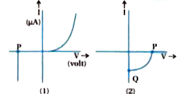
(i) Name the type of a diode whose characteristics are shown in figure (1) and figure (2).
(ii) What does the point P in figure (1) represent?
(iii) What does the points P and Q in figure (2) represent?
View SolutionThe conductivity of a semiconductor increases with increase in temperature because
View SolutionTwo charges –q and +q are located at points (0, 0, –a) and (0, 0, a), respectively.
(a) What is the electrostatic potential at the points (0, 0, z) and (x, y, 0) ?
(b) Obtain the dependence of potential on the distance r of a point from the origin when r/a>>1 .
(c) How much work is done in moving a small test charge from the point (5,0,0) to (–7,0,0) along the x-axis? Does the answer change if the path of the test charge between the same points is not along the x-axis?
View SolutionAccording to particle theory of light what is the velocity of light in a dense medium, compared to that in rare medium ?
View SolutionIn the depletion region of a diode.
View SolutionIn the depletion region of an unbiased p-n junction diode there are
View SolutionWhat is 'depletion region' in a semiconductor diode?
View SolutionWhat is 'depletion region' in a semiconductor diode?
View Solutionp-n सन्धि डायोड के अवक्षय क्षेत्र में
View SolutionIn the depletion region of an unbiased p-n junction diode, there are
View SolutionIn the depletion region of the an unbaised p-n junction diode, there are
View SolutionWhat is 'depletion region' in a semiconductor diode?
View Solutionनिम्न में से कौन-सा कथन किसी डायोड के अवक्षय क्षेत्र (Depletion region) के लिए सही नहीं है?
View Solutionकिसी pn संधि डायोड में अवक्षय क्षेत्र की चौड़ाई
View Solution
