To get light in visible region through LED …….. Semiconductor is used. Solution in Gujrati
silicon
germanium
gallium
tellurium
The correct Answer is:C
Step by step video, text & image solution for To get light in visible region through LED …….. Semiconductor is used. by Physics experts to help you in doubts & scoring excellent marks in Class 12 exams.
Topper's Solved these Questions
- BOOK - KUMAR PRAKASHANCHAPTER - SEMICONDUCTOR ELECTRONICS : MATERIALS, DEVICES AND SIMPLE CIRCUITS EXERCISE - Section-D : Multiple Choice Questions (MCQs) (MCQs asked in Competitive Exams)129videos
SEMICONDUCTOR ELECTRONICS : MATERIALS, DEVICES AND SIMPLE CIRCUITS
- BOOK - KUMAR PRAKASHANCHAPTER - SEMICONDUCTOR ELECTRONICS : MATERIALS, DEVICES AND SIMPLE CIRCUITS EXERCISE - Section-C: NCERT Exemplar Solution (Long Answer Type Questions)10videos
SEMICONDUCTOR ELECTRONICS : MATERIALS, DEVICES AND SIMPLE CIRCUITS
- BOOK - KUMAR PRAKASHANCHAPTER - SAMPLE QUESTION PAPER EXERCISE - PART-B SECTION-C5videos
SAMPLE QUESTION PAPER
- BOOK - KUMAR PRAKASHANCHAPTER - WAVE OPTICSEXERCISE - SECTION-D (MULTIPLCE CHOICE QUESTIONS (MCQS)) (MCQS FROM DARPAN BASED ON TEXTBOOK)239videos
WAVE OPTICS
Similar Questions
At absolute zero temperature Si acts as ……..
01:40View Solution
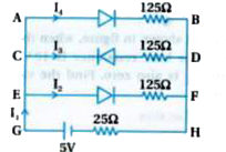
If each diode in figure has a forward bias resistance of 25Ω and infinite resistance in reverse bias, what will be the values of the current I1,I2,I3andI4?01:46View SolutionTwo charges –q and +q are located at points (0, 0, –a) and (0, 0, a), respectively.
(a) What is the electrostatic potential at the points (0, 0, z) and (x, y, 0) ?
(b) Obtain the dependence of potential on the distance r of a point from the origin when r/a>>1 .
(c) How much work is done in moving a small test charge from the point (5,0,0) to (–7,0,0) along the x-axis? Does the answer change if the path of the test charge between the same points is not along the x-axis?01:18View SolutionAccording to particle theory of light what is the velocity of light in a dense medium, compared to that in rare medium ?
01:31View SolutionExplain why elemental semiconductor cannot be used to make visible LEDs.
01:25View SolutionMention the important considerations required while fabricating a p-n junction diode to be used as light emitting diode (LED). What should be the order of the band gap of an LED if it is required to emit light in the visible region.
02:37View SolutionAssertion: The semiconductor used for fabrication of visible LEDs must at least have a band gap of 1.8 eV.
Reason: The spectral range of visible light is 0.4 eV to 1.8 eV06:47View SolutionIn LED visible light is produced by
02:43View Solutionप्रकाश उत्सर्जक डायोड (LED ) बनाने के लिए उपयोग में लिए जाने वाले किसी एक अपमिश्रित अर्द्धचालक का नाम लिखिए।
01:37View SolutionFor LEDs to emit light in visible region of electromagnetic light it should have energy band gap in the range of
03:06View Solutionस्पष्ट कीजिए कि तात्विक अर्द्धचालकों का उपयोग दृश्य LED बनाने में क्यों नहीं किया जा सकता?
01:34View Solutionदृश्य फोटॉनों की ऊर्जाओं का परास (लगभग ) 1.8 eV से 2.8 eV तक होता है। इस सुचना के प्रयोग से तर्क दें कि क्यों दृश्य प्रकाश LED डिज़ाइन करने के लिए सिलिकॉन, उपयुक्त अर्धचालक नहीं है ?
01:21View SolutionExplain why elemental semiconductor cannot be used to make visible LEDs.
View SolutionExplain why elemental semiconductor cannot be used to make visible LEDs.
02:03View SolutionMention the important considerations required while fabricating a p-n junction diode to be used as light emitting diode (LED). What should be the order of the band gap of an LED if it is required to emit light in the visible region.
02:22View Solution

