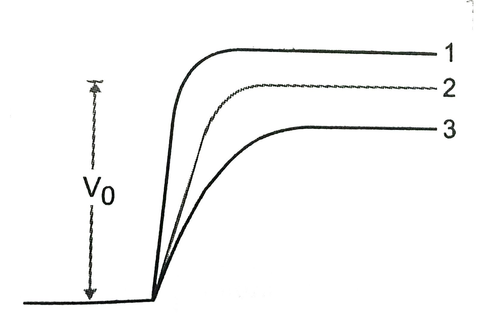
In forward bias, the width of potential barrier in a P−N junction diode
increases
decreases
remains constant
first increases then decreases
The correct Answer is:B
To solve the question regarding the behavior of the potential barrier width in a P-N junction diode when it is forward biased, we can follow these steps:
1. Understanding P-N Junction Diode:
- A P-N junction diode consists of two types of semiconductor materials: P-type (positive) and N-type (negative). The junction between these two types creates a region known as the depletion region, which has a potential barrier.
2. Forward Bias Configuration:
- In forward bias, the P-type side is connected to the positive terminal of the battery, and the N-type side is connected to the negative terminal. This configuration allows current to flow through the diode.
3. Effect of Forward Bias on the Potential Barrier:
- When the diode is forward biased, the external voltage reduces the potential barrier created by the depletion region. This is because the positive voltage on the P-side repels holes towards the junction, while the negative voltage on the N-side repels electrons towards the junction.
4. Change in Width of the Potential Barrier:
- As the potential barrier decreases due to the applied forward bias, the width of the depletion region (or potential barrier) also decreases. This allows more charge carriers (holes and electrons) to recombine across the junction, facilitating current flow.
5. Conclusion:
- Therefore, in forward bias, the width of the potential barrier in a P-N junction diode decreases.
Final Answer:
- The width of the potential barrier in a P-N junction diode in forward bias decreases.
- A P-N junction diode consists of two types of semiconductor materials: P-type (positive) and N-type (negative). The junction between these two types creates a region known as the depletion region, which has a potential barrier.
- In forward bias, the P-type side is connected to the positive terminal of the battery, and the N-type side is connected to the negative terminal. This configuration allows current to flow through the diode.
- When the diode is forward biased, the external voltage reduces the potential barrier created by the depletion region. This is because the positive voltage on the P-side repels holes towards the junction, while the negative voltage on the N-side repels electrons towards the junction.
- As the potential barrier decreases due to the applied forward bias, the width of the depletion region (or potential barrier) also decreases. This allows more charge carriers (holes and electrons) to recombine across the junction, facilitating current flow.
- Therefore, in forward bias, the width of the potential barrier in a P-N junction diode decreases.
- The width of the potential barrier in a P-N junction diode in forward bias decreases.
Similar Questions
The cause of the potential barrier in a p-n diode is:
View SolutionThe increase in the width of the depletion region in a p-n junction diode is due to:
View SolutionFor a reverse bias P-N junction-
View SolutionIn a forward biased PN- junction diode, the potential barrier in the depletion region is of the from...
View SolutionThe barrier potential in a P-N junction is maximum in
View SolutionIn forward biasing of the p-n junction:
View SolutionHow is forward biasing different from reverse biasing in a p-n junction diode?
View SolutionIn p-n junction diode, near junction holes combine with electrons, and impurity ions form a barrier potential which opposes the recombination of electron-hole pairs. Value of barriers potential for Si is 0.7 volt and for Ge is 0.3 V. thus charge density at the junction becomes zero and an electric field is produced near junction. this region is called depletion layer. Thickness of depletion layer is of the order of 10−6 meter. in forward bias p terminal is connected with the positive terminal of cell and n is connected with negative terminal of cell and n is connected with negative terminal of cell. as forward voltage is increased, current increases exponentially.
As forward voltage is increased barrier potential in p-n junction diode is
A. increased
B. Decreased
C. remain same
D. nothing can be said.
View SolutionReverse bias applied to a junction diode
View SolutionIn Fig . V0 is the potential barrier across a p-n junction, when no battery is connected across the junction

View Solution
