In junction diode, the holes are due to
protons
extra electrons
neutrons
missing eletrons
The correct Answer is:D
To solve the question "In junction diode, the holes are due to," we need to understand the concept of holes in semiconductor physics.
1. Understanding the Structure of Silicon:
- Silicon (Si) is a semiconductor with four valence electrons. In its crystalline form, each silicon atom forms covalent bonds with four neighboring silicon atoms.
2. Doping Silicon:
- To create a p-type semiconductor, we introduce a trivalent impurity, such as aluminum (Al), into the silicon crystal. Trivalent means that aluminum has three valence electrons.
3. Formation of Holes:
- When aluminum is added to silicon, it forms bonds with three silicon atoms. However, since aluminum has only three valence electrons, it cannot form a bond with the fourth silicon atom. This results in a missing electron in the crystal structure.
4. Concept of Holes:
- The absence of an electron in the bonding structure is referred to as a "hole." Therefore, in a p-type semiconductor, holes are created due to the missing electrons that result from the trivalent doping.
5. Conclusion:
- In a junction diode, the holes are due to missing electrons created by the introduction of trivalent impurities (like aluminum) into the silicon crystal. Thus, the correct answer is "missing electrons."
Final Answer:
The holes in a junction diode are due to missing electrons.
---
- Silicon (Si) is a semiconductor with four valence electrons. In its crystalline form, each silicon atom forms covalent bonds with four neighboring silicon atoms.
- To create a p-type semiconductor, we introduce a trivalent impurity, such as aluminum (Al), into the silicon crystal. Trivalent means that aluminum has three valence electrons.
- When aluminum is added to silicon, it forms bonds with three silicon atoms. However, since aluminum has only three valence electrons, it cannot form a bond with the fourth silicon atom. This results in a missing electron in the crystal structure.
- The absence of an electron in the bonding structure is referred to as a "hole." Therefore, in a p-type semiconductor, holes are created due to the missing electrons that result from the trivalent doping.
- In a junction diode, the holes are due to missing electrons created by the introduction of trivalent impurities (like aluminum) into the silicon crystal. Thus, the correct answer is "missing electrons."
The holes in a junction diode are due to missing electrons.
Similar Questions
Knowledge Check
In a p−n junction diode, the barrier potential opposes diffusion of
Aminority carrier in both regions onlyBmajority carriers onlyCelectrons in p regionDholes in p region
In a p-n junction,a potential barrier of 250 mev exsists across the junction.A hole with a kimetic energy of 300 meV approaches the junction. Find the kinetic energy of the hole when it crosses the junction if the hole approached the junction (a)from the p-side and (b)from the n-side.
View SolutionBarrier potential of a p−n junction diode does not depend on
View SolutionBarrier potential of a p−n junction diode does not depend on
View SolutionIn a p-n junction diode the value of drift current through depletion region
View SolutionIn a forward biased PN- junction diode, the potential barrier in the depletion region is of the from...
View SolutionChoose the correct option:
At equilibrium in a p-n junction diode the net current is
(A) due to diffusion of majority charge carriers
(B) due to drift of minority charge carriers
(C) zero as diffusion and drift currents are equal and opposite
(D) zero as no charge carriers cross the junction
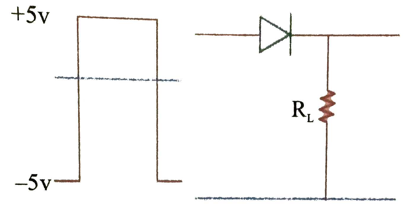
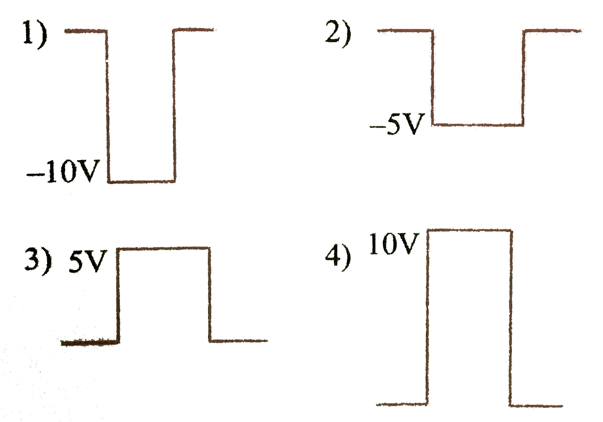
View SolutionIf a p−n junction diode, a square input signal of 10V is applied as shown.

Then the out put signal across RL will be
 .
.
View Solution
