In a semiconductor diode p-side is earthed and N-side is applied a potential of -2V, the diode shall
Conduct
Not conduct
Conduct partially
Break down
The correct Answer is:A
To solve the question regarding the behavior of a semiconductor diode when the p-side is earthed and the n-side is applied a potential of -2V, we can follow these steps:
1. Identify the Configuration:
- The p-side of the diode is earthed, which means it is at 0 volts.
- The n-side is applied a potential of -2 volts.
2. Determine the Voltages:
- Let’s denote the voltage at the p-side (VA) as 0V (since it is earthed).
- The voltage at the n-side (VB) is -2V.
3. Compare the Voltages:
- We need to compare VA and VB:
- VA = 0V (p-side)
- VB = -2V (n-side)
- Since VA (0V) is greater than VB (-2V), we have:
- VA > VB.
4. Analyze the Biasing Condition:
- In a p-n junction diode, if the p-side is at a higher potential than the n-side, the diode is said to be in forward bias.
- In this case, since VA > VB, the diode is forward biased.
5. Conclusion:
- A forward-biased diode allows current to flow through it. Therefore, the diode will conduct electricity.
Final Answer:
The diode shall conduct (Option 1).
---
- The p-side of the diode is earthed, which means it is at 0 volts.
- The n-side is applied a potential of -2 volts.
- Let’s denote the voltage at the p-side (VA) as 0V (since it is earthed).
- The voltage at the n-side (VB) is -2V.
- We need to compare VA and VB:
- VA = 0V (p-side)
- VB = -2V (n-side)
- Since VA (0V) is greater than VB (-2V), we have:
- VA > VB.
- In a p-n junction diode, if the p-side is at a higher potential than the n-side, the diode is said to be in forward bias.
- In this case, since VA > VB, the diode is forward biased.
- A forward-biased diode allows current to flow through it. Therefore, the diode will conduct electricity.
The diode shall conduct (Option 1).
Topper's Solved these Questions
- SEMICONDUCTOR ELECTRONICS (MATERIAL, DEVICES AND SIMPLE CIRUITS )BOOK - AAKASH INSTITUTE ENGLISHCHAPTER - SEMICONDUCTOR ELECTRONICS (MATERIAL, DEVICES AND SIMPLE CIRUITS )EXERCISE - Assignment section -B (Objective Type Question)
29 Videos
- SEMICONDUCTOR ELECTRONICS (MATERIAL, DEVICES AND SIMPLE CIRUITS )BOOK - AAKASH INSTITUTE ENGLISHCHAPTER - SEMICONDUCTOR ELECTRONICS (MATERIAL, DEVICES AND SIMPLE CIRUITS )EXERCISE - Assignment section -C (Previous years type question)
110 Videos
- SEMICONDUCTOR ELECTRONICS (MATERIAL, DEVICES AND SIMPLE CIRUITS )BOOK - AAKASH INSTITUTE ENGLISHCHAPTER - SEMICONDUCTOR ELECTRONICS (MATERIAL, DEVICES AND SIMPLE CIRUITS )EXERCISE - EXERCISE
20 Videos
- RAY OPTICS AND OPTICAL INSTRUMENTSBOOK - AAKASH INSTITUTE ENGLISHCHAPTER - RAY OPTICS AND OPTICAL INSTRUMENTSEXERCISE - ASSIGNMENT (SECTION - D)
16 Videos
- SEMICONDUCTOR ELECTRONICS: MATERIALS, DEVICES AND SIMPLE CIRCUITSBOOK - AAKASH INSTITUTE ENGLISHCHAPTER - SEMICONDUCTOR ELECTRONICS: MATERIALS, DEVICES AND SIMPLE CIRCUITSEXERCISE - Assignment (Section-D (Assertion and reason))
5 Videos
Similar Questions
In a semiconductor diode, what is meant by potential barrier ?
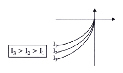
View SolutionIdentify the semiconductor diode whose I-V characters is as shown:
View SolutionWith reference to a semiconductor diode, define the terms .depletion region. and .potential barrier.. How will the width of depletion region change during reverse biasing?
View SolutionReverse bias applied to a junction diode
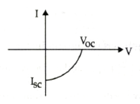
View SolutionIdentify the semiconductor diode whose I-V characteristics as shown:
View SolutionFind the power loss in each diode (in mW), if potential drop across the zener diode is 8V
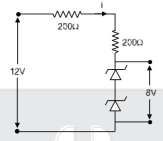
View SolutionFind the power loss in each diode (in mW), if potential drop across the zener diode is 8V

View SolutionIn a semiconductor diode, reserve bias current is due to drift of free electrons and holes caused by
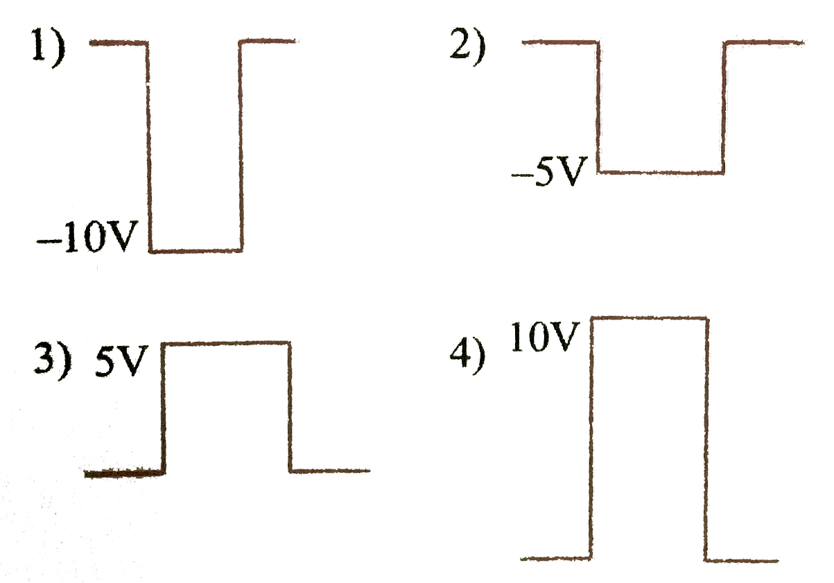
View SolutionIf a p−n junction diode, a square input signal of 10V is applied as shown.
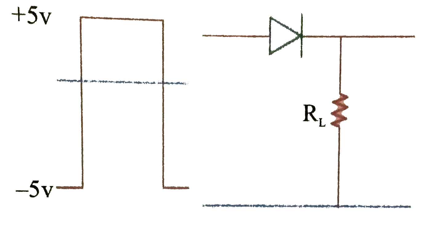
Then the out put signal across RL will be
 .
.
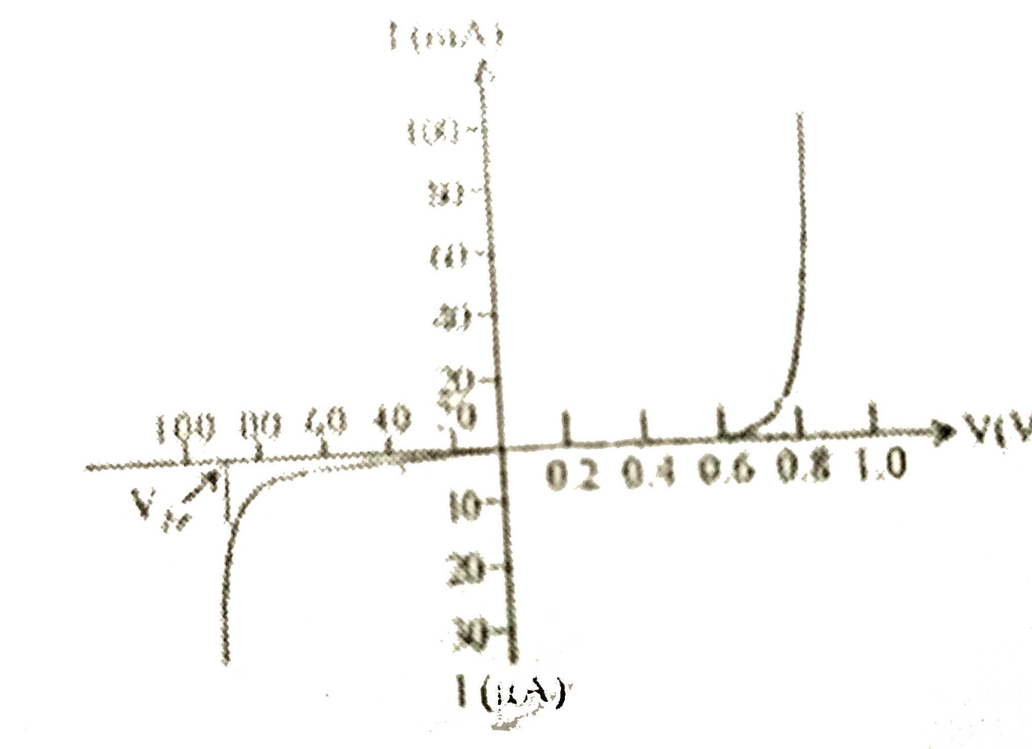
View SolutionThe figure below shows the V-I characteristic of a semiconductor diode.
(i ) Identify the semiconductor diode used.
(ii) Draw the circuit diagram to obtain the given characteristic of this device.
(ii) Briefly explain how this diode can be used as a voltage regulator.
View Solution
