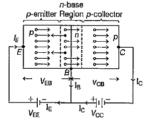
Describe the construction and working of a p-n-p transitor with necessary circuit diagram. Establish the relation among the transistor parameters .
Text Solution
p-n-p transistor From figure ,we can see that the emitter -base junction is reverse biased as shown in figure below.
 The resistance of emitter -base junction is very low So , the voltage of VEE(VEB) is quite small (i.e .1,5V). The current in p-n-p transistor is carried by holes and at the same time their concentration is maintained . But in external circuit the current is due to the flow of electrons .
In this case , IE=IB+IC [using Kirchhoff. s law ] (11/2)
Re7lation between 7transistor parameters
(i) Relation between αandβ
As , ΔIE=ΔIB+ΔIC
⇒ΔIEΔIC=ΔIBΔIC+1
⇒1α=1β+1
∴β=α1−αorα=β1+β
Relation between αandγ
As, ΔIE=ΔIB+ΔIC
⇒1=ΔIBΔIE+ΔICΔIE
⇒1=1γ+α
⇒α=γ−1γ
(iii) Relation between βandγ
As ΔIE=ΔIB+ΔIC
⇒ΔIEΔIB=1+ΔICΔIB
γ=1+β
|
Similar Questions
Knowledge Check
In a p-n-p transistor, the n-type crystal works as a
AgateBbaseCcollectorDemitterActive state of n-p-n transistor, in circuit is achieved by
ALow input voltageBHigh input voltageCBoth (low input voltage) and (high input voltage)DNeither (low input voltage) nor (high input voltage)Active state of n-p-n transistor, in circuit is achieved by
Alow input voltageBhigh input voltageCboth a and bDNeither a nor b
In p-n-p transistor, what are the current carriers inside and output the transistor circuit?
View SolutionDescribe briefly the functions of the three segments of n-p-n transistor.
View SolutionDraw the symbol of a p-n-p transistor. Show the biasing of a p-n-p transistor and explain the transistor action.
View SolutionDescribe briefly with the help of a necessary circuit diagram, the working principle of a solar cell.
View Solution(i) Draw a circuit diagram to study the input and output characteristics of an n-p-n transistor in its common emitter configuration. Draw the typical input and output characteristics.
(ii) Explain, with the hepl of a circuit diagram, the working of n-p-n transistor as a common emitter amplifier.
View Solution
