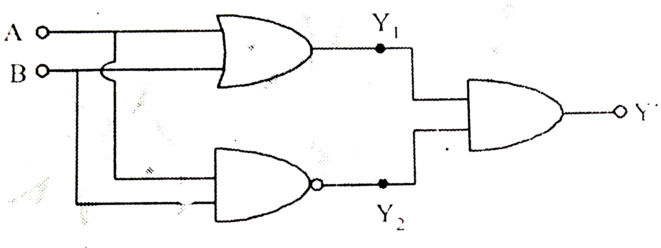
The following configuration of gate is equivalent to

A
NAND gate
B
XOR gate
C
OR gate
D
NOR gate.
Video Solution
Text Solution
The correct Answer is:B

Y1=A+B,Y2=¯¯¯¯¯¯¯¯A.B
Y=(A+B).¯¯¯¯¯¯¯¯A.B=¯¯¯¯¯¯¯¯A.A+¯¯¯¯¯¯¯¯A.B+¯¯¯¯¯¯¯¯B.A+¯¯¯¯¯¯¯¯B.B
=0+¯¯¯¯¯¯¯¯A.B+¯¯¯¯¯¯¯¯B.A+0=¯¯¯¯¯¯¯¯A.B=¯¯¯¯¯¯¯¯B.A
This expression is for XOR.
|
Similar Questions
Knowledge Check
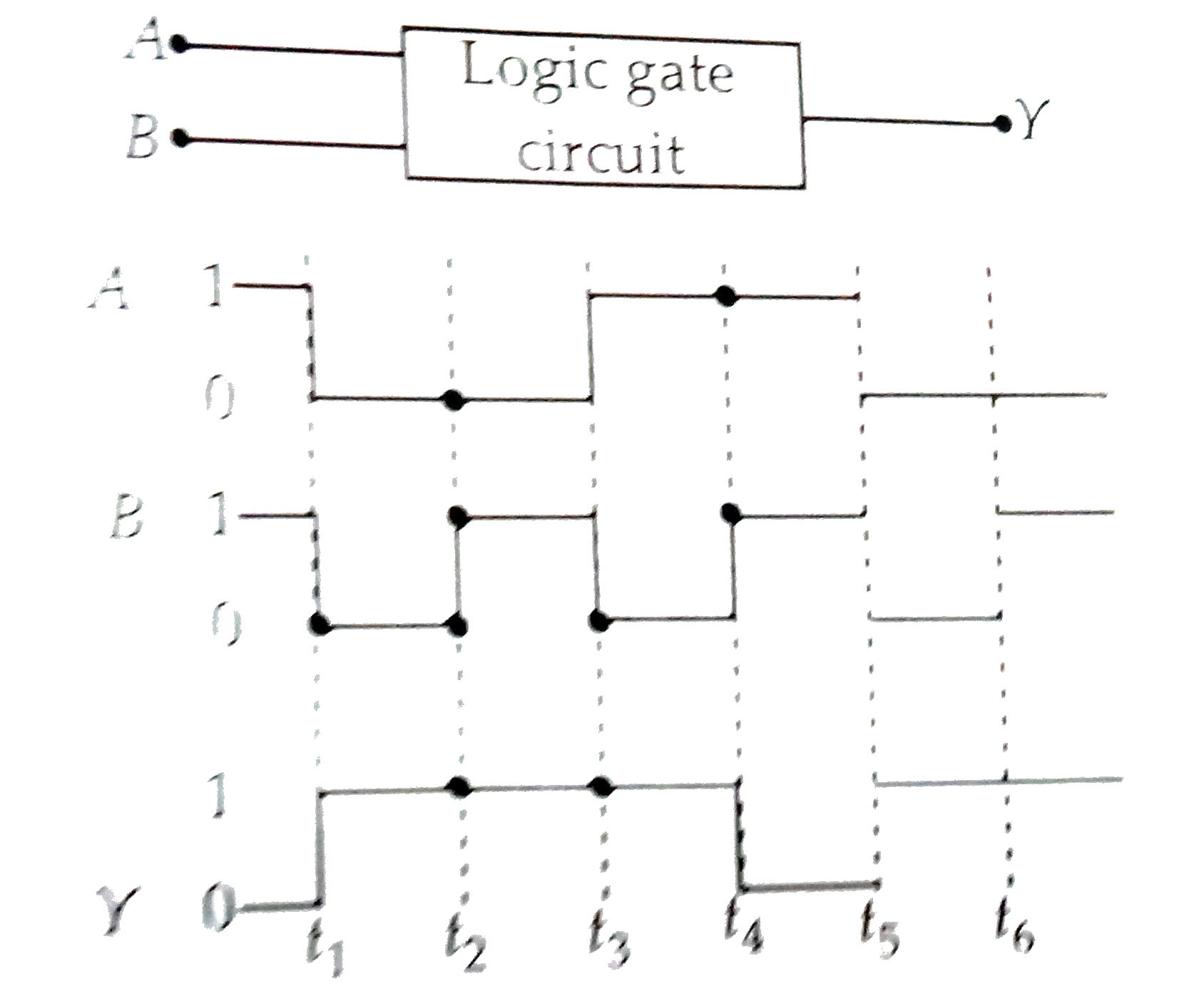
The following figure shows a logic gate circuit with two inputs A and B and the output Y. The voltage waveforms of A,B and Y are as given :

The logic gate isANOR gateBOR gateCAND gateDNAND gate
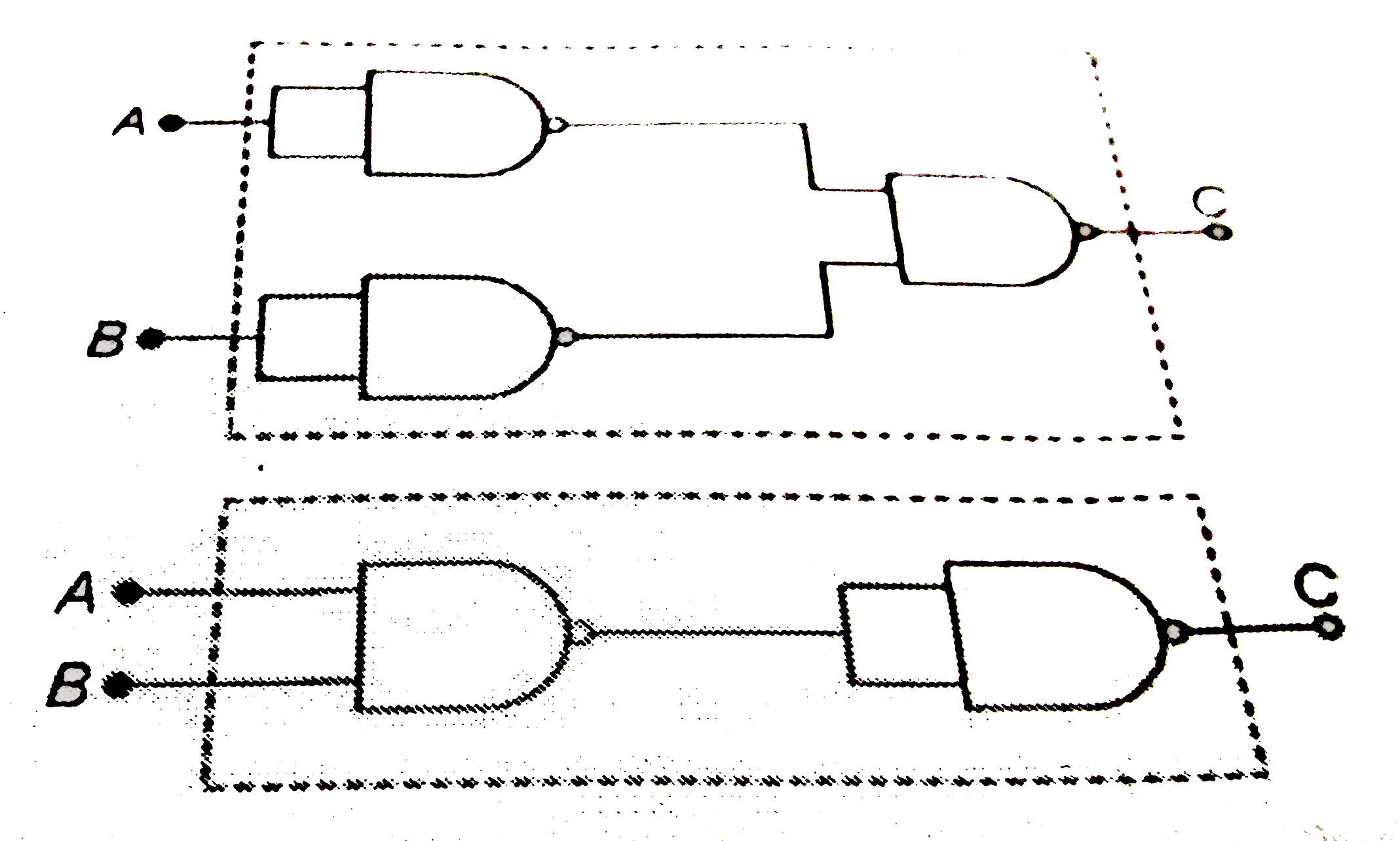
Which of the following configuration is not possible ?
View SolutionThe truth table for the following combination of gates is :-
_E01_430_Q01.png)
View SolutionThe combination of gates shown here are equivalent to

View SolutionWhich of the following configuration is incorrect ?
View SolutionWhich of the following configuration is incorrect ?
View SolutionWhich of the following configurations is incorrect?
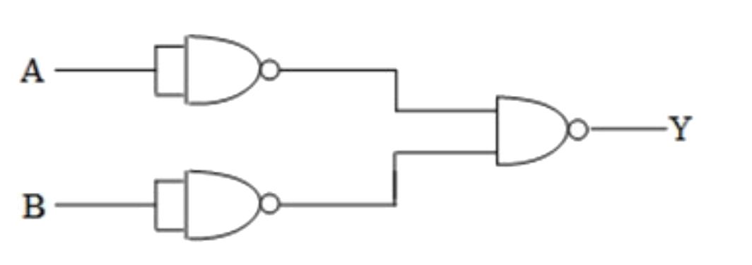
View SolutionFollowing circuit is equivalent to

View Solution

_2019_CBT4_E01_066_Q01.png)
