p-n junction is said to be forward biased, when
positive terminal of the battery is connected to the p-type semiconductor and negative is connected to the n-type semiconductor
positive terminal of battery is connected to the n-type semiconductor and negative terminal is connected to the p-type semiconductor
positive terminal of battery is connected to the n-type of semiconductor
a mechanical force is applied in forward direction
The correct Answer is:A
Step by step video solution for p-n junction is said to be forward biased, when by Physics experts to help you in doubts & scoring excellent marks in Class 11 exams.
Updated on:21/07/2023Topper's Solved these Questions
- SEMICONDUCTORSBOOK - ALLENCHAPTER - SEMICONDUCTORSEXERCISE - Part-3(Exercise-2)
49 Videos
- SEMICONDUCTORSBOOK - ALLENCHAPTER - SEMICONDUCTORSEXERCISE - Part-3(Exercise-3)
27 Videos
- SEMICONDUCTORSBOOK - ALLENCHAPTER - SEMICONDUCTORSEXERCISE - Part-3(Exercise-4)
51 Videos
- PHYSICAL WORLD, UNITS AND DIMENSIONS & ERRORS IN MEASUREMENT BOOK - ALLENCHAPTER - PHYSICAL WORLD, UNITS AND DIMENSIONS & ERRORS IN MEASUREMENT EXERCISE - EXERCISE-IV
8 Videos
- WAVES AND OSCILLATIONSBOOK - ALLENCHAPTER - WAVES AND OSCILLATIONSEXERCISE - Part-1(Exercise-05)[B]
42 Videos
Similar Questions
Knowledge Check
A forward biased diode is
A B
B C
C D
D
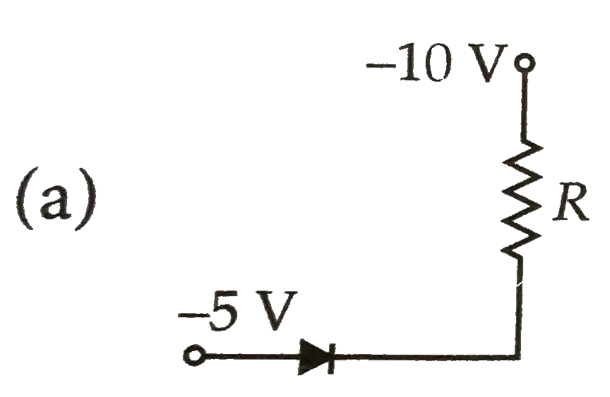
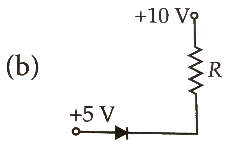
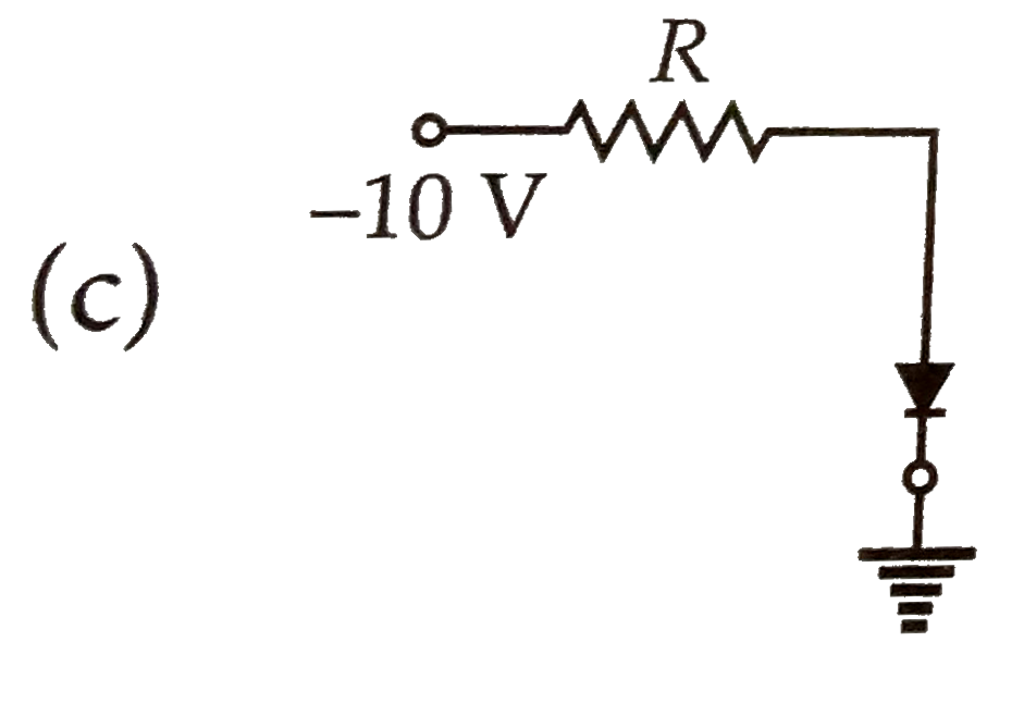
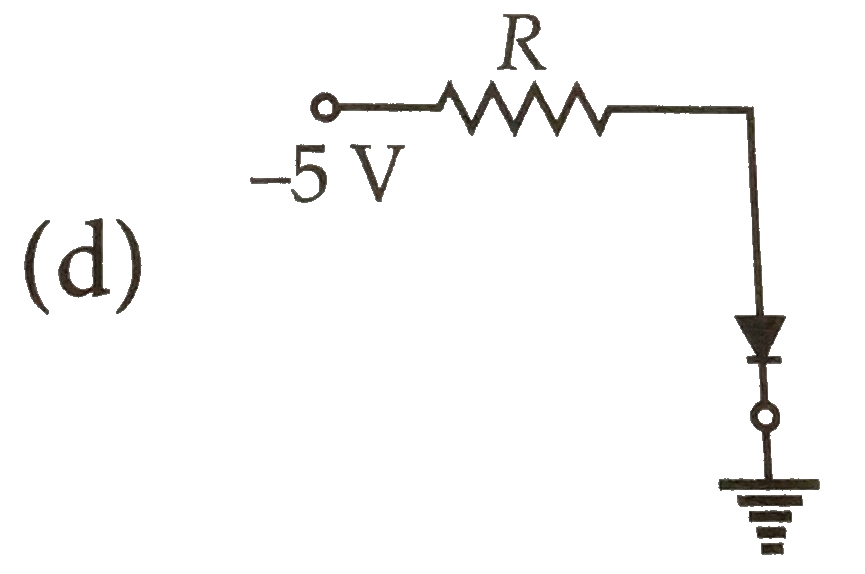
Which of the junction diodes shown below are forward biased ?
A B
B C
C D
D
When p−n junction diode is forward biased then
View SolutionWhen p−n junction diode is forward biased then
View SolutionWhat happens to the width of depletion layer of a p-n junction when it is (i) forward biased, (ii) reverse biased?
View SolutionUsing the necessary circuit diagram, show how the V-I characteristics of a p-n junction are obtained in (i) forward biasing (ii) Reverse biasing. How are these characteristics made use of in rectification?
View SolutionA p-n junction in series with a resistance of 5kΩ is connected across a 50 V DC source . If the forward bias resistance of the junction is 50Ω , the forward bias current is
View Solution(a) Explain with the help of suitable diagram , the two processes which occur during the formations of a p -n junction diode . Hence , define the terms :
(i) depletion region and (ii) potential barrier :
(b) Draw a circuit diagram of a p - n junction diode under forward bias and explain its working .
View Solution