The barrier potentials for silicon and Germanium diodes are about
0.7V , 0.3V
0.2V, 0.3 volts
1.1V, 0.7V
1.1V , 0.3V
The correct Answer is:A
Step by step video & image solution for The barrier potentials for silicon and Germanium diodes are about by Physics experts to help you in doubts & scoring excellent marks in Class 12 exams.
Topper's Solved these Questions
- BOOK - AAKASH SERIESCHAPTER - SEMICONDUCTOR DEVICESEXERCISE - EXERCISE -I (TRANSISTORS)22videos
SEMICONDUCTOR DEVICES
- BOOK - AAKASH SERIESCHAPTER - SEMICONDUCTOR DEVICESEXERCISE - EXERCISE -I (LOGIC GATES)17videos
SEMICONDUCTOR DEVICES
- BOOK - AAKASH SERIESCHAPTER - SEMICONDUCTOR DEVICESEXERCISE - EXERCISE -I (ENERGY BANDS AND CLASSIFICATION OF SOLIDS )41videos
SEMICONDUCTOR DEVICES
- BOOK - AAKASH SERIESCHAPTER - RAY OPTICSEXERCISE - PROBLEMS ( LEVEL-II)60videos
RAY OPTICS
- BOOK - AAKASH SERIESCHAPTER - UNITS AND MEASUREMENTEXERCISE - PRACTICE EXERCISE45videos
UNITS AND MEASUREMENT
Similar Questions
Knowledge Check
- Question 1 - Select One
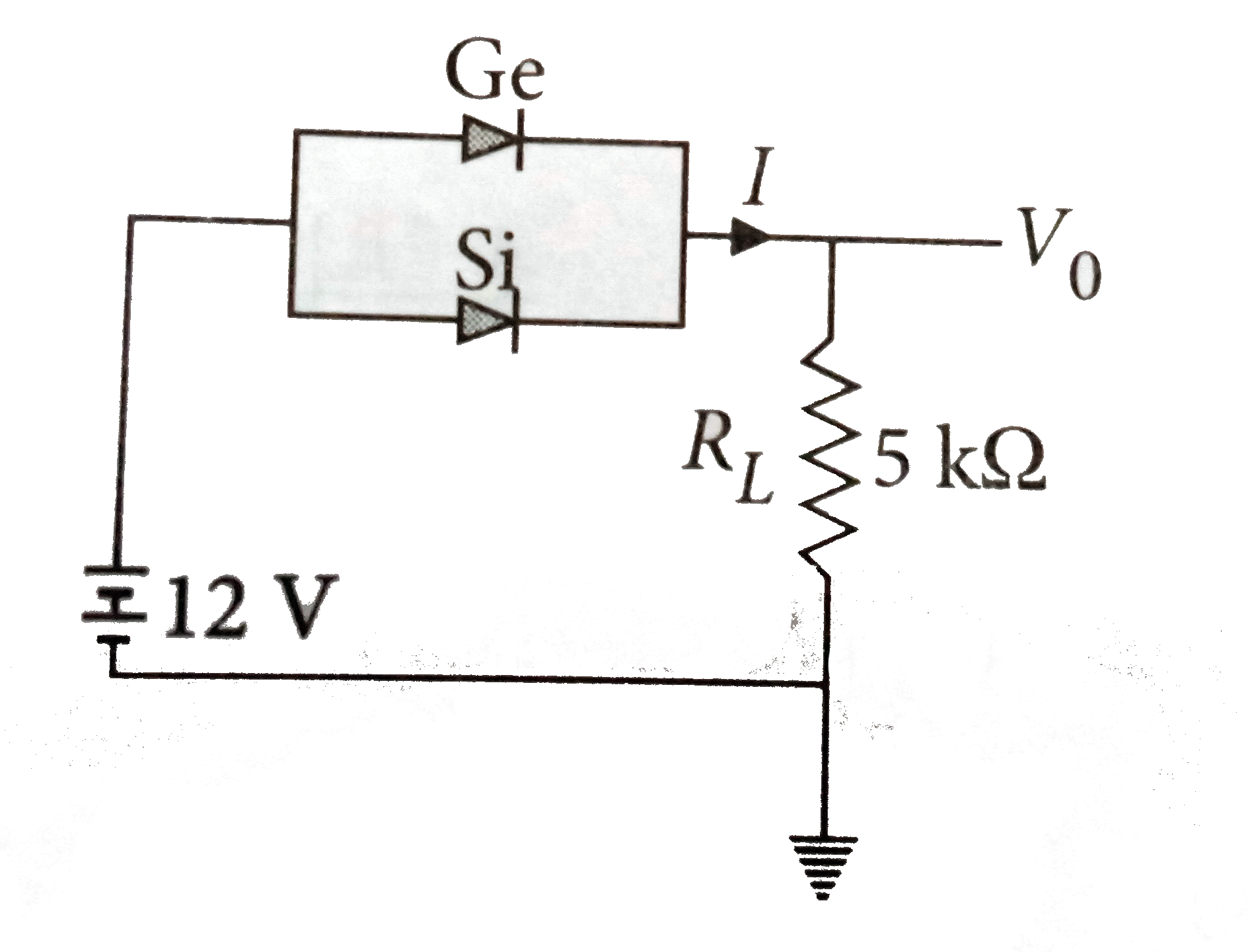
In the circuit shown in figure, the silicon and germanium diodes start conducting at 0.7 V and 0.3 V respectively. What are the values of V0 and I?
 A12 V, 2.4 mAB11.7 V, 2.34 mAC11.3 V, 2.26 mAD11 V, 2.2 mA
 - Question 2 - Select One
Germanium is an example of
Aintrinsidc semiconductorBn-type semiconductorCp-type semiconductorDinsulator.
The value of barrier potential of P-N juntion in Ge is-
View SolutionSilicones are
View SolutionWhy are elemental dopants for Silicon or Germanium usually chosen from group XIII or group XV?
View SolutionIn p-n junction diode, near junction holes combine with electrons, and impurity ions form a barrier potential which opposes the recombination of electron-hole pairs. Value of barriers potential for Si is 0.7 volt and for Ge is 0.3 V. thus charge density at the junction becomes zero and an electric field is produced near junction. this region is called depletion layer. Thickness of depletion layer is of the order of 10−6 meter. in forward bias p terminal is connected with the positive terminal of cell and n is connected with negative terminal of cell and n is connected with negative terminal of cell. as forward voltage is increased, current increases exponentially.
As forward voltage is increased barrier potential in p-n junction diode is
A. increased
B. Decreased
C. remain same
D. nothing can be said.View SolutionThe energy gaps (Eg) between valence band and conduction band for diamond, silicon and germanium are in the order
View SolutionWhen the reverse potential in a semiconductor diode are 10 V and 30 V, thent he corresponding reverse currents are 25μA. And 50μA respectively. The reverse resistance of junction diode will be-
View Solution

