Consider the folllowing statements i and ii and identify the correct choice of the given answers.
A zener diode is always connected in reverse bias.
The potential barrier of a p-n junction lies between 0.03 to 0.1 V approximately.
A and B are correct
A and B are wrong
A is correct but B is wrong
A is wrong but B is correct
The correct Answer is:C
Step by step video, text & image solution for Consider the folllowing statements i and ii and identify the correct choice of the given answers. A zener diode is always connected in reverse bias. The potential barrier of a p-n junction lies between 0.03 to 0.1 V approximately. by Physics experts to help you in doubts & scoring excellent marks in Class 12 exams.
Updated on:21/07/2023Topper's Solved these Questions
- ELECTRONICSBook:ERRORLESSChapter:ELECTRONICSExercise:NCERT Based Questions (Junction Transistor)
Explore 29 Videos
- ELECTRONICSBook:ERRORLESSChapter:ELECTRONICSExercise:NCERT Based Questions (Digital Electronics)
Explore 23 Videos
- ELECTRONICSBook:ERRORLESSChapter:ELECTRONICSExercise:Assertion & Reason
Explore 26 Videos
- ELECTRON, PHOTON, PHOTOELECTRIC EFFECT & X -RAYBook:ERRORLESSChapter:ELECTRON, PHOTON, PHOTOELECTRIC EFFECT & X -RAYExercise:ASSERTION & REASON
Explore 27 Videos
- ELECTROSTATICSBook:ERRORLESSChapter:ELECTROSTATICSExercise:ASSERTION & REASON
Explore 25 Videos
Similar Questions
Draw the V-I characterisitics of p-n junction diode in forward bias and in reverse bias.
View Solutionp-n junction is a semiconductor diode. It is obtained by bringing p-type semiconductor inclose contact with n-type semiconductor. A thin layer is developed at the p-n junction which is devoid of any charge carrier but has immobile ions. It is called depletion layer. At the junction a potential barrier appears, which does not allow the movement of majority charge carriers across the junction in the absence of any biasing of the junction.
p-n junction offer low resistance when forward biased and high resistance when reverse biased. Read the above paragaph and answer the following question:
(i) Can we measure the potential barrier of p-n junction by putting a sensitive voltmeter across its terminals?
(ii) What practical lesson do you draw from the above study?
View Solution
Knowledge Check
Consider the folllowing statements i and ii and identify the correct choice of the given answers.
A zener diode is always connected in reverse bias.
The potential barrier of a p-n junction lies between 0.1 to 0.03 V approximately.Ai and ii are correctBi and ii are wrongCi is correct but ii is wrongDi is wrong but ii is correct.Consider the following statements A and B and identify the correct answer
(A) A Zener diode is always connected in reverse bias to use it as voltage regulator.
(B) The potential barrier of a p−n junction lies between 0.1 to 0.3V, approximately.AA and B are correctBA and B are wrongCA is correct but B is wrongDA is wrong but B is correct.Consider the following statements A and B and identify the correct answer.
(A)A zener diode should be connected in reverse bias for proper functioning
(B) The potential barrier of a p-n junction lies between 2 V and 5 VABoth A and B are correctBBoth A and B are wrongCA is wrong and B is correctDA is correct but B is wrong
Consider the following statement A and B and identify the correct choice of the given answers
A: The width of the depletion layer in a P−N junction diode increases in forwards biase
B: In an intrinsic semiconductor the fermi energy level is exactely in the middle of the forbidden gap
View SolutionConsider the following statements A and B. Identify for correct in the given answer.
A) p−n,p−p,n−n forces between nucleons are not equal and charge dependent.
B) In nuclear reactor the fission reaction will be in accelerating state if the value of neutron reproduction factor K>1
View SolutionConsider the following statements A and B and identify the correct answer
(1) : Germanium is preferred over silicon in the construction of zener diode.
(2) : Germanium has high thermal stability than silicon in the construction of Zener diode.
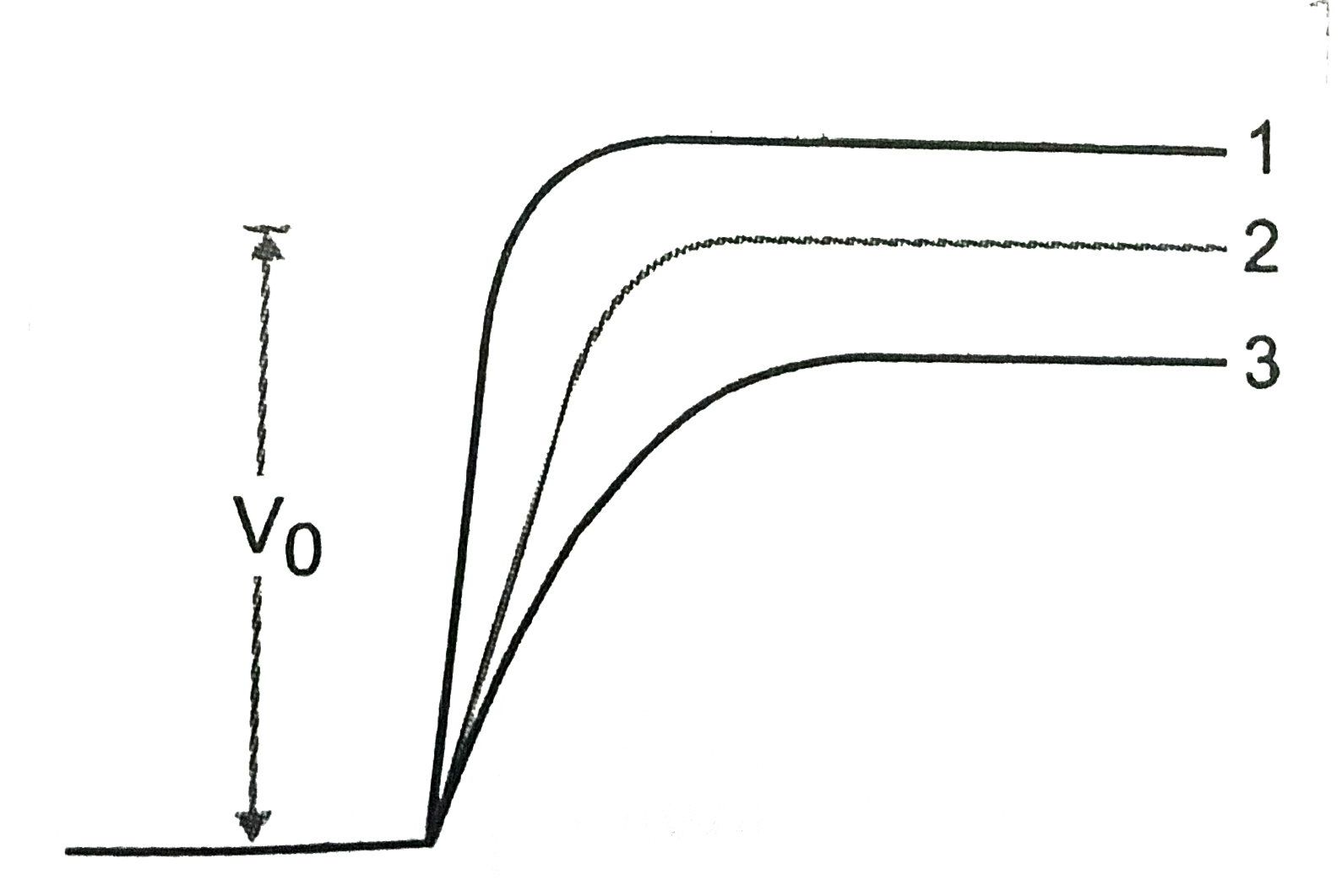
View SolutionIn Fig . V0 is the potential barrier across a p-n junction, when no battery is connected across the junction

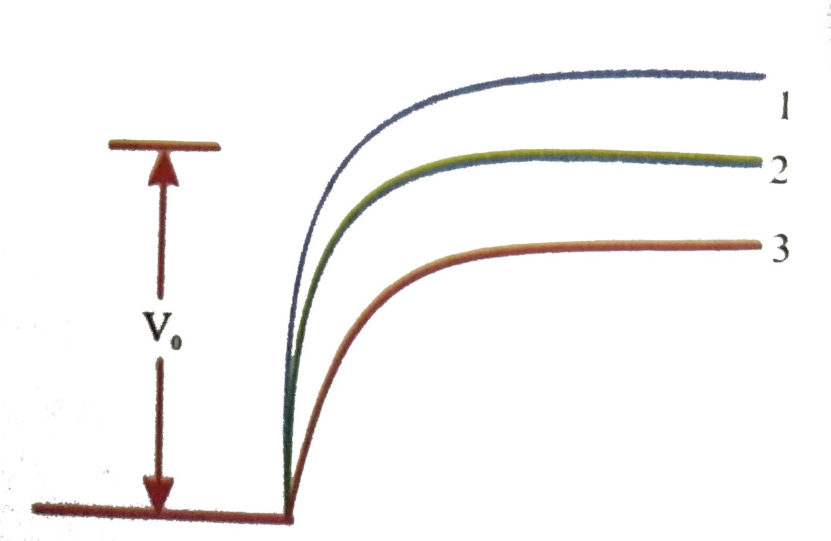
View SolutionIn Fig. V0 is the potential barrier across a p−n junction, when no battery is connected across the junction :
 .
.
View Solution